Smart medical
Introduction: Technical challenges and SiC opportunities of smart healthcare
With the deep integration of artificial intelligence, the Internet of Things and big data, smart medical care is rapidly advancing the precision of diagnosis, intelligent equipment and remote service. However, this process places greater demands on the performance of medical devices:
High efficiency: the equipment needs to run stably for a long time to ensure real-time data processing and transmission;
Low energy consumption: reducing hospital operating costs in response to the global Green Healthcare initiative;
Miniaturization: Portable devices need to balance battery life and functional integration.
Silicon carbide (SiC) semiconductors, with their inherent advantages of wide band gap materials, are the core solution to break these technical bottlenecks and are reshaping the future of medical electronic devices.
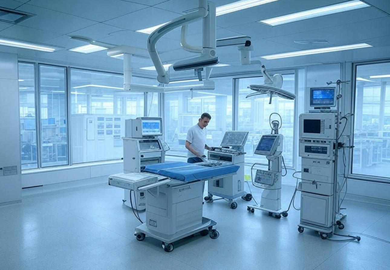
The core application scenario of SiC in smart medical treatment
1. Medical imaging equipment: the "power heart" for accurate diagnosis
CT/MRI High Voltage Generator:
SiC power devices increase the power conversion efficiency of imaging devices to 98%, reducing energy waste while reducing device operating noise and improving the patient experience.
Ultrasonic probe power supply system:
SiC chip is used to optimize power supply stability, improve image resolution, and help identify early lesions.
2. Surgical robot: The "nerve center" of precise operation
Minimally invasive surgical robotic arm:
The high response speed and low delay characteristics of the SiC drive module ensure that the action error of the robot arm is less than 0.1 mm, reducing the risk of fine operations such as vascular suture.
Energy Platform Equipment:
SiC based high frequency electrotome can reduce tissue carbonization and accelerate postoperative recovery.
3. Wearable and telemedicine devices: "Invisible guards" of health monitoring
Heart Monitor:
The low power consumption of the SiC chip extends the battery life of the device by 30% and supports 72 hours of continuous ECG monitoring.
Portable dialysis machine:
With SiC power module, the weight is reduced by 20%, which is convenient for patients to use at home.
4. Medical power system: the "energy cornerstone" of green hospitals
Data center and laboratory power supply:
The SiC inverter can reduce the overall energy consumption of the hospital by 15% and reduce carbon emissions by more than 100 tons per year.
Emergency Power Supply (UPS) :
High reliability SiC devices ensure 0 ms switching of the backup power supply when the operating room is powered off, safeguarding the safety of patients.
Future Outlook: How does SiC define the next generation of smart healthcare?
Ai-driven Predictive maintenance:
SiC devices have built-in sensors that monitor device status in real time, combined with AI algorithms to predict failures and reduce the risk of downtime.
Globalization of remote surgery:
Ultra-low delay surgical robots supported by 5G+SiC technology will break regional restrictions and realize trans-continental sharing of expert resources.
Nanoscale implantable devices:
The biocompatibility and miniaturization potential of SiC provide new possibilities for implantable devices such as smart insulin pumps and nerve stimulators.
4. Industry case: SiC technology landing practice
Siemens Healthcare: Uses SiC power modules in new MRI systems to increase scanning speed by 25% and reduce energy consumption by 18%.
Intuitive Surgical: The next generation Da Vinci surgical robot integrates a SiC drive unit to improve surgical accuracy to the micron level.
Conclusion: SiC semiconductor - the invisible engine of smart medical treatment
From improving diagnostic accuracy to reducing the global medical carbon footprint, SiC semiconductors are quietly driving a medical technology revolution. With the explosive growth of global demand for efficient and green medical care, SiC technology will become the core competitiveness of medical device manufacturers and medical institutions. Embracing SiC is not only a choice for technology upgrading, but also a responsible commitment to life health and sustainable development