Quartz Wafer 6-Inch High Purity Double-Side Polished Substrate: Precision Engineered for Semiconductor and Optical Excellence
Introduction
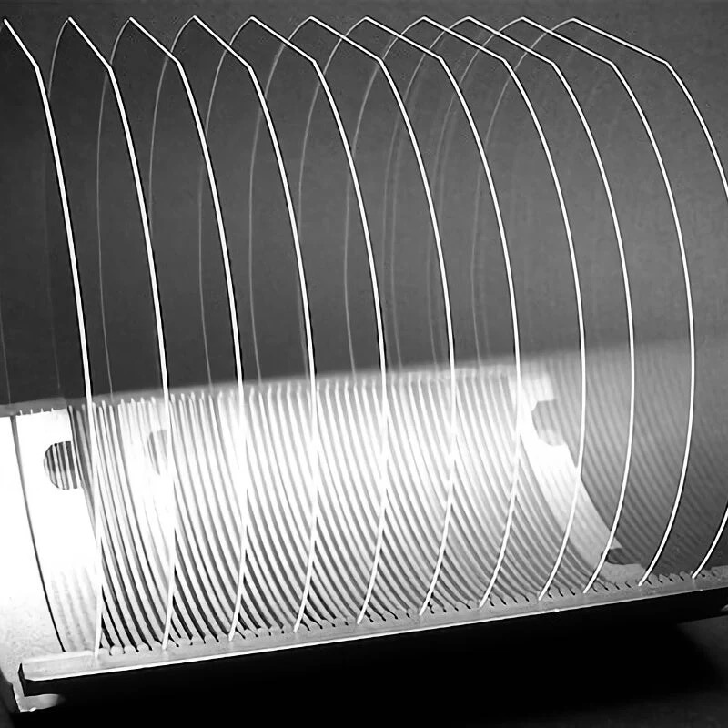
In the high-stakes world of semiconductor manufacturing and advanced optics, substrate quality is a cornerstone of success. The Quartz Wafer 6-Inch High Purity Double-Side Polished Substrate is engineered to meet the rigorous demands of cutting-edge technologies. Crafted from synthetic fused silica (SiO₂) with atomic-level precision, this substrate delivers unparalleled purity, thermal resilience, and optical performance, making it indispensable for EUV lithography, MEMS devices, and high-energy laser systems.
Key Features
Ultra-High Purity (99.999% SiO₂)
Synthetic fused silica with metallic impurities <1 ppm, ensuring contamination-free processes for EUV lithography and sensitive optical applications.Double-Side Polished Perfection
Both surfaces polished to <0.5 nm (Ra) roughness, enabling flawless thin-film deposition, lithography, and optical coatings.Exceptional Thermal Stability
Near-zero thermal expansion (CTE: 0.55 × 10⁻⁶/°C) maintains dimensional integrity at temperatures up to 1,200°C.Broad Optical Transparency
High transmittance (>90%) from UV (190 nm) to IR (2,500 nm), ideal for deep-UV lithography, laser optics, and space-grade sensors.Chemical and Plasma Resistance
Resists acids, alkalis, and plasma etching, ensuring durability in harsh semiconductor and cleanroom environments.SEMI-Compliant Standards
Meets SEMI specifications for flatness (<3 µm TTV), thickness uniformity (±10 µm), and defect density, compatible with 150mm fab tools.
Applications
Semiconductor Lithography: EUV/DUV photomasks for sub-5nm chip production.
MEMS & Sensors: Precision substrates for accelerometers, gyroscopes, and biochips.
Advanced Optics: Lenses, prisms, and beam splitters for high-power lasers and telescopes.
Quantum Technologies: Photonic circuits and qubit arrays in quantum computing systems.
Aerospace & Defense: IR-transparent windows, radomes, and satellite sensor protection.
Why Choose a 6-Inch Quartz Substrate?
Yield Optimization: Ultra-smooth surfaces minimize defects in EUV patterning and thin-film processes.
Scalability: 6-inch (150mm) format aligns with industry standards for cost-effective high-volume production.
Future-Ready Design: Supports next-gen innovations like 3D IC integration and integrated photonics.
Cost Efficiency: Reusable and durable, reducing long-term operational costs.
Regulatory Compliance: Certified to SEMI, ISO, and MIL-STD standards for quality assurance.
Conclusion
The 6-inch Quartz Wafer High Purity Double-Side Polished Substrate is a critical enabler of precision in semiconductor, optical, and quantum industries. Its unmatched purity, thermal stability, and atomic-level surface quality empower manufacturers to achieve breakthroughs in miniaturization, efficiency, and performance. For engineers and researchers pushing the boundaries of technology, this substrate is the foundation of tomorrow’s innovations.