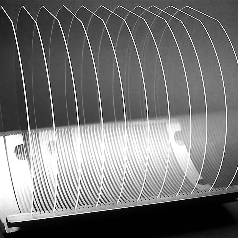
Quartz Wafer 8-Inch High Purity Double-Side Polished Substrate: Precision for Advanced Semiconductor and Optical Applications
Introduction
As semiconductor and photonic technologies advance toward smaller nodes and higher precision, the demand for larger, ultra-pure substrates grows. The Quartz Wafer 8-Inch High Purity Double-Side Polished Substrate addresses this need, offering unmatched material quality, dimensional stability, and surface precision. Crafted from synthetic fused silica (SiO₂), this substrate is a cornerstone for EUV lithography, optical systems, and MEMS manufacturing. This article explores its features, applications, and why it is critical for next-generation innovations.
Key Features
Ultra-High Purity (99.999% SiO₂)
Synthetic fused silica with metallic impurities <1 ppm, ensuring contamination-free processes in EUV lithography and high-energy optics.Double-Side Polished Precision
Both surfaces polished to <0.5 nm (Ra) roughness, enabling defect-free patterning, thin-film deposition, and optical coatings.Exceptional Thermal Stability
Near-zero thermal expansion (CTE: 0.55 x 10⁻⁶/°C), maintaining dimensional integrity under extreme temperatures (up to 1,200°C).Broad Optical Transparency
High transmittance (>90%) across UV (190 nm) to IR (2,500 nm) spectra, ideal for deep-UV lithography and laser optics.Chemical and Plasma Resistance
Withstands aggressive acids, alkalis, and plasma environments, ensuring durability in semiconductor fabrication and cleaning cycles.SEMI-Compliant Standards
Meets SEMI specifications for flatness (<3 µm TTV), thickness uniformity (±10 µm), and defect density, compatible with 200mm fab tools.
Applications
EUV Lithography: Photomask substrates for sub-3nm semiconductor node production.
Advanced Optics: Lenses, prisms, and beam splitters for high-power laser systems and space telescopes.
MEMS and Sensors: Precision substrates for accelerometers, gyroscopes, and biochips.
Quantum Technologies: Base material for photonic circuits and qubit arrays in quantum computing.
Aerospace & Defense: IR-transparent windows, radomes, and sensor protection in extreme environments.
Why Choose an 8-Inch Quartz Substrate?
Scalability: Larger 8-inch (200mm) format aligns with industry standards for high-volume semiconductor production.
Yield Optimization: Ultra-smooth surfaces reduce defects in EUV mask patterning and thin-film processes.
Future-Ready Design: Supports emerging technologies like 3D IC integration and integrated photonics.
Cost Efficiency: High durability and reusability lower total cost of ownership.
Regulatory Compliance: Certified for traceability and quality under SEMI, ISO, and MIL-STD standards.
Conclusion
The 8-inch Quartz Wafer High Purity Double-Side Polished Substrate is a pivotal enabler of innovation in semiconductor and photonic industries. Its unparalleled purity, thermal resilience, and atomic-level surface precision empower manufacturers to push the limits of miniaturization and performance. Whether for EUV lithography, quantum devices, or aerospace optics, this substrate delivers the reliability and precision required to lead in a competitive technological landscape.