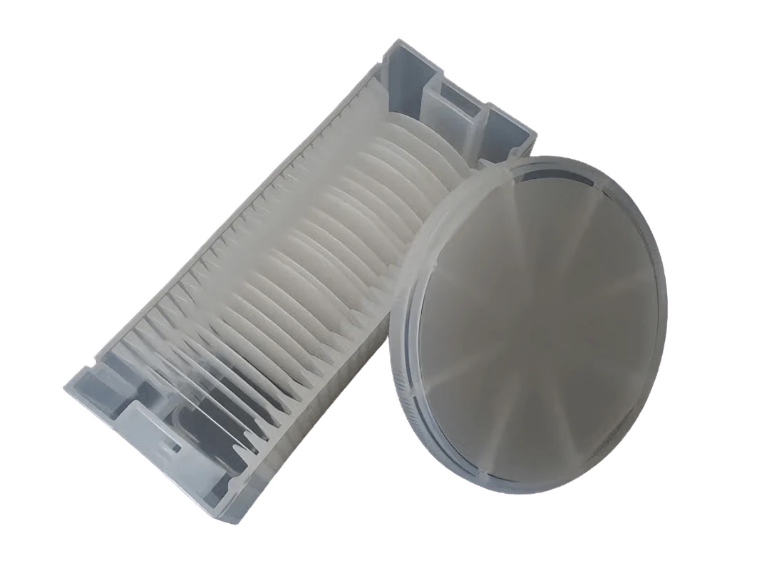
Sapphire Wafer 6-Inch High Purity LED Optics Double-Side Polished Substrate: Precision for High-Performance Optoelectronics
Introduction
In the pursuit of high-efficiency optoelectronic devices, the quality of substrate materials directly impacts performance and reliability. The Sapphire Wafer 6-Inch High Purity Double-Side Polished Substrate stands at the forefront of innovation, offering unparalleled surface smoothness, thermal resilience, and crystal integrity. Designed for demanding applications like GaN-based LEDs, laser systems, and high-power electronics, this substrate combines large-format scalability with precision engineering to meet the needs of modern manufacturing.
Key Features
Ultra-High Purity (99.99%)
Synthetic sapphire (Al₂O₃) with impurity levels <10 ppm, ensuring minimal defects and optimal light transmission for high-brightness LEDs and optical devices.Double-Side Polished Precision
Both surfaces polished to <0.3 nm (Ra) roughness, enabling flawless epitaxial growth, lithography, and optical coatings for enhanced device performance.Superior Thermal Management
High thermal conductivity (35 W/m·K) and resistance to extreme temperatures (up to 1,800°C), ideal for MOCVD processes and high-power applications.Crystal Orientation Options
Available in C-plane, M-plane, or R-plane orientations to support diverse applications like non-polar GaN growth, RF devices, and SAW filters.Chemical and Mechanical Durability
Resists acids, alkalis, and mechanical stress, ensuring longevity in aggressive fabrication environments.SEMI-Compliant Standards
Meets SEMI specifications for flatness (<3 µm TTV), thickness tolerance (±15 µm), and defect density, compatible with automated production lines.
Applications
High-Brightness LEDs: Substrate for GaN epitaxy in automotive lighting, displays, and industrial illumination.
Laser Diodes & VCSELs: Precision base for telecom, LiDAR, and medical laser systems.
Optical Sensors: Windows for UV/IR detection in aerospace, environmental monitoring, and healthcare.
Power Electronics: Insulating substrates for high-voltage RF devices and semiconductor packaging.
Emerging Technologies: Quantum computing, micro-LEDs, and integrated photonic circuits.
Why Choose a 6-Inch Double-Side Polished Sapphire Substrate?
Scalability: Larger 6-inch format aligns with 150mm fab standards, reducing costs for high-volume production.
Enhanced Yield: Ultra-smooth surfaces minimize defects in epitaxial layers and optical coatings.
Versatility: Supports dual-side processing for advanced device architectures and optical applications.
Future-Ready: Drives innovation in next-gen technologies like AR/VR displays and 5G infrastructure.
Cost Efficiency: High durability and process compatibility lower total cost of ownership.
Conclusion
The 6-inch Sapphire Wafer Double-Side Polished Substrate is a cornerstone of optoelectronic advancement, combining precision, purity, and scalability. Its exceptional thermal stability and surface quality empower manufacturers to achieve higher efficiencies, brighter outputs, and longer device lifespans. For industries pushing the boundaries of LED technology, laser systems, and beyond, this substrate delivers the reliability and performance needed to lead in a competitive market.


