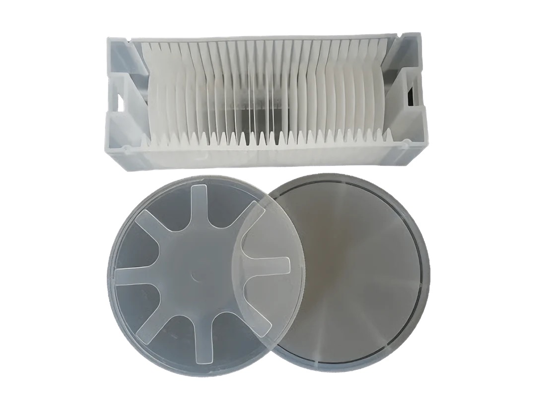
Sapphire Wafer 2-Inch M/A/R-Plane High Purity LED Optics Single-Side Polished Substrate: Precision for Cutting-Edge Optoelectronics
Introduction
In the rapidly evolving optoelectronics industry, crystal orientation is a critical factor in optimizing device performance. The Sapphire Wafer 2-Inch M/A/R-Plane High Purity Single-Side Polished Substrate is engineered to meet the demands of advanced LED, laser diode, and semiconductor applications. With precise M-plane (1-100), A-plane (11-20), or R-plane (1-102) orientations, this substrate enables superior epitaxial growth, reduced polarization effects, and enhanced light extraction. This article explores its features, applications, and why it’s a strategic choice for next-generation technologies.
Key Features
Custom Crystal Orientations
M-Plane (1-100): Enables non-polar GaN epitaxy, reducing efficiency droop in high-brightness LEDs.
A-Plane (11-20): Ideal for anisotropic device designs in RF and specialized optics.
R-Plane (1-102): Used in surface acoustic wave (SAW) devices and heteroepitaxial growth.
Ultra-High Purity (99.99%)
Synthetic sapphire (Al₂O₃) with impurity levels <10 ppm, ensuring defect-free epitaxial layers and high optical clarity.Single-Side Polished Precision
Polished surface roughness <0.5 nm (Ra), optimized for thin-film deposition and lithography. Unpolished backside ensures mechanical stability during processing.Thermal and Chemical Resilience
Withstands temperatures up to 1,800°C (MOCVD-ready) and offers high thermal conductivity (35 W/m·K).
Resists acids, alkalis, and plasma etching for durability in harsh fabrication environments.
SEMI-Compliant Standards
Meets SEMI specifications for flatness (<5 µm TTV), thickness tolerance (±10 µm), and defect density.Compact and Versatile
2-inch (50.8mm) diameter with thickness options from 430µm to 1,000µm, ideal for R&D prototyping and niche production.
Applications
High-Efficiency LEDs: M-plane substrates for non-polar GaN LEDs in automotive and display lighting.
Laser Diodes: A-plane for edge-emitting lasers in LiDAR and telecom systems.
RF and SAW Devices: R-plane substrates for high-frequency filters and sensors.
Optical and UV Sensors: Windows for industrial, medical, and aerospace monitoring.
Quantum and Photonic R&D: Prototyping advanced devices like micro-LEDs and photonic circuits.
Why Choose M/A/R-Plane Sapphire Substrates?
Eliminate Polarization: M-plane enhances LED efficiency by reducing electric field-induced droop.
Anisotropic Control: A/R-plane supports specialized mechanical and optical device designs.
Cost-Effective Prototyping: Smaller 2-inch format minimizes material waste for research and low-volume production.
Future-Ready: Enables innovations in 5G, AR/VR, and quantum computing.
SEMI Compliance: Ensures compatibility with automated fabrication and inspection tools.
Conclusion
The 2-inch M/A/R-Plane Sapphire Wafer is a versatile, high-performance substrate tailored for advanced optoelectronics. Its precision crystal orientations, ultra-smooth surface, and thermal resilience empower engineers to push the boundaries of LED efficiency, laser diode performance, and RF device innovation. For researchers and manufacturers prioritizing customization and cutting-edge quality, this substrate is a cornerstone of technological progress.


