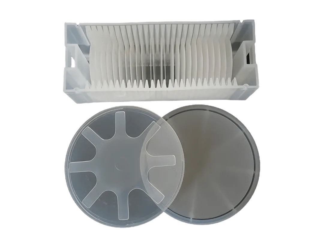
Sapphire Wafer 4-Inch M/A-Plane High Purity LED Optics Single-Side Polished Substrate: Precision for Advanced Optoelectronics
Introduction
In the quest for superior optoelectronic performance, crystal orientation plays a pivotal role in device efficiency and functionality. The Sapphire Wafer 4-Inch M/A-Plane High Purity Single-Side Polished Substrate is engineered to meet the demands of advanced LED, laser diode, and semiconductor applications requiring precise crystal alignment. With its M-plane or A-plane orientation and ultra-smooth polished surface, this substrate enables tailored epitaxial growth, enhanced light extraction, and robust thermal management. This article delves into its features, applications, and why it’s a strategic choice for cutting-edge optoelectronics.
Key Features
M/A-Plane Crystal Orientation
M-Plane (1-100): Ideal for non-polar GaN epitaxy, reducing polarization effects in LEDs and laser diodes.
A-Plane (11-20): Suited for specialized applications requiring anisotropic mechanical and optical properties.
Ultra-High Purity (99.99%)
Synthetic sapphire (Al₂O₃) with minimal impurities (<10 ppm), ensuring high transparency and defect-free epitaxial growth.Single-Side Polished Precision
Polished surface roughness <0.5 nm (Ra), optimized for high-quality thin-film deposition and lithography. The unpolished backside provides mechanical stability during processing.Exceptional Thermal and Chemical Resistance
Thermal conductivity: 35 W/m·K, withstanding temperatures up to 1,800°C (MOCVD-ready).
Resists acids, alkalis, and plasma etching, ensuring durability in harsh fabrication environments.
SEMI-Compliant Standards
Meets SEMI specifications for flatness (<5 µm TTV), thickness tolerance (±10 µm), and defect density, ensuring compatibility with automated production tools.Customizable Dimensions
4-inch (100mm) diameter with thickness options from 430µm to 1,000µm, tailored for R&D prototyping or high-volume manufacturing.
Applications
Non-Polar LED Production: M-plane substrates reduce efficiency droop in high-brightness LEDs for displays and automotive lighting.
Laser Diodes: A-plane sapphire supports edge-emitting lasers for telecommunications and LiDAR systems.
High-Frequency Electronics: M/A-plane’s anisotropic properties benefit RF devices and power electronics.
Optical Sensors: Substrates for UV/IR sensors in aerospace, medical, and industrial monitoring.
Research & Innovation: Prototyping quantum devices, photonic circuits, and advanced MEMS.
Why Choose M/A-Plane Sapphire Substrates?
Eliminate Polarization Effects: M-plane enables non-polar GaN growth, enhancing LED efficiency and color consistency.
Tailored Anisotropy: A-plane supports specialized device designs requiring directional mechanical/optical properties.
Scalability: Larger 4-inch format reduces material waste and aligns with industry-standard fabrication tools.
Future-Ready: Drives advancements in micro-LEDs, VCSELs, and next-gen photonic integration.
Cost Efficiency: High durability and process compatibility lower total cost of ownership.
Conclusion
The 4-inch M/A-Plane Sapphire Wafer Single-Side Polished Substrate is a game-changer for optoelectronic engineers seeking precision, versatility, and performance. Its unique crystal orientation, ultra-smooth surface, and SEMI compliance make it indispensable for applications demanding reduced polarization, anisotropic control, and thermal resilience. Whether for high-efficiency LEDs, advanced lasers, or emerging quantum technologies, this substrate empowers innovation in a competitive technological landscape.


