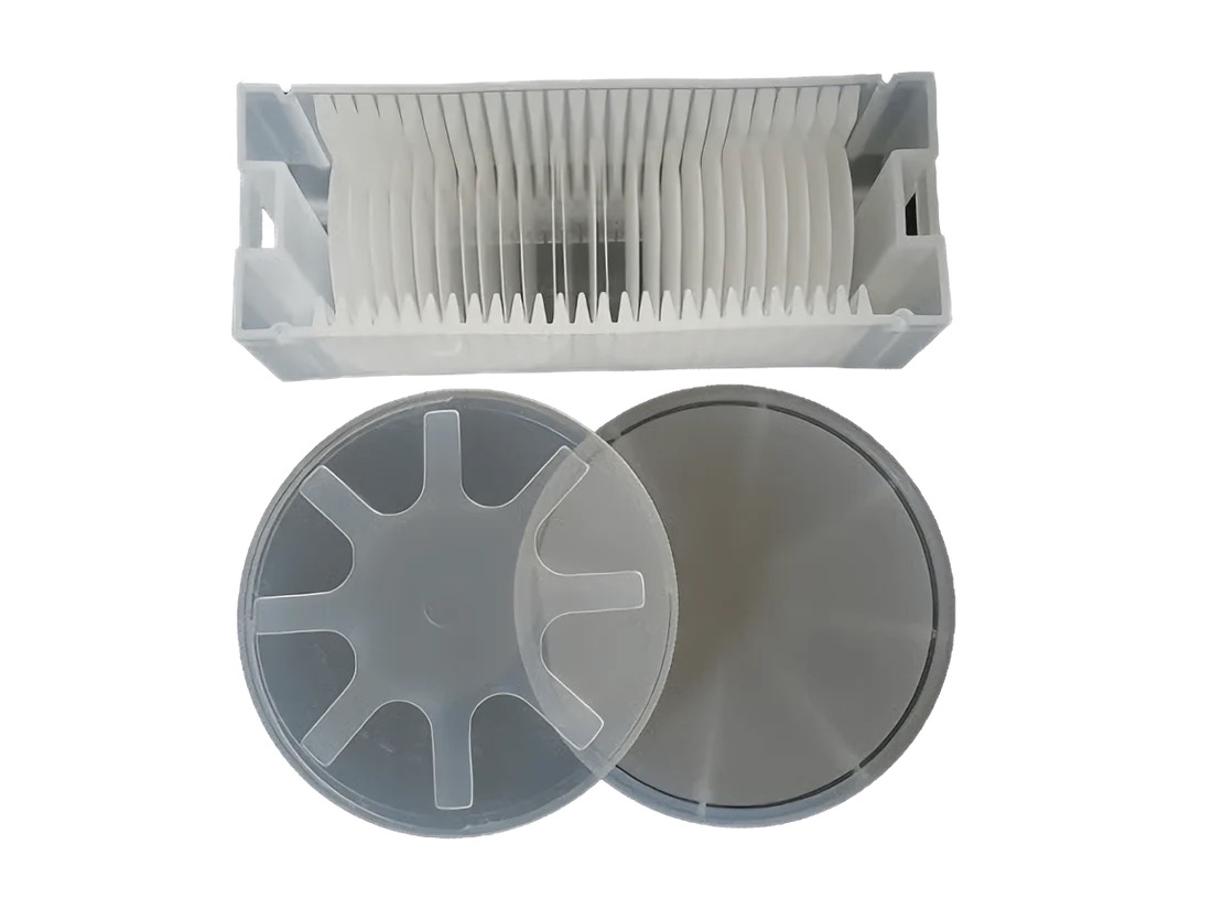
Sapphire Wafer 2-Inch C-Plane High-Purity LED Optics Single-Side Polished Substrate: Precision for Optoelectronic Innovation
Introduction
In the fast-evolving world of optoelectronics and LED manufacturing, substrate quality directly impacts device performance and longevity. The Sapphire Wafer 2-Inch C-Plane High-Purity Single-Side Polished Substrate stands as a critical enabler of cutting-edge LED and laser technologies. Engineered with a C-plane orientation and ultra-smooth polished surface, this substrate ensures optimal epitaxial growth, light extraction, and thermal management for high-brightness LEDs and beyond. This article explores its features, applications, and why it’s a top choice for optoelectronic engineers.
Key Features
C-Plane Crystal Orientation
Precisely aligned (0001) C-plane structure, ideal for gallium nitride (GaN) epitaxial growth in LED and laser diode fabrication.High Purity (99.99%)
Synthetic sapphire (Al₂O₃) with minimal impurities (<10 ppm), ensuring high light transmission and reduced defects in optoelectronic devices.Single-Side Polished Precision
Polished surface roughness <0.5 nm (Ra), minimizing light scattering and enhancing LED luminous efficiency. Unpolished backside supports mechanical stability during processing.Exceptional Thermal Stability
High thermal conductivity (35 W/m·K) and resistance to temperatures up to 1,800°C, critical for MOCVD and high-power LED processes.Chemical and Mechanical Durability
Resists acids, alkalis, and abrasion, ensuring longevity in harsh fabrication environments.Standardized Dimensions
2-inch (50.8mm) diameter with thickness options from 430µm to 1,000µm, compatible with industry-standard handling and epitaxy tools.
Applications
High-Brightness LEDs: Substrate for GaN-based LEDs in displays, automotive lighting, and general illumination.
Laser Diodes: Base material for blue/violet laser diodes in Blu-ray, LiDAR, and medical devices.
Power Electronics: RF and high-voltage devices leveraging sapphire’s insulating properties.
Optical Sensors: Windows and substrates for UV/IR sensors in industrial and aerospace systems.
Research & Prototyping: Cost-effective solution for developing next-gen optoelectronic technologies.
Why Choose C-Plane Sapphire Substrates?
Enhanced Epitaxial Quality: C-plane alignment promotes uniform GaN growth, boosting LED brightness and yield.
Optical Efficiency: Ultra-smooth polished surface maximizes light extraction and minimizes losses.
Cost Efficiency: Smaller 2-inch format reduces material waste for prototyping and niche production.
Industry Compliance: Meets SEMI standards for flatness, purity, and defect density.
Versatility: Compatible with PVD, CVD, and photolithography processes.
Conclusion
The 2-inch C-Plane Sapphire Wafer is a cornerstone of optoelectronic innovation, combining crystal precision, thermal resilience, and optical excellence. Its single-side polished design and high purity make it indispensable for manufacturers aiming to push the boundaries of LED efficiency, laser performance, and semiconductor reliability. For engineers prioritizing quality and scalability in optoelectronics, this substrate delivers unmatched value in a competitive market.


