Quartz Wafer Diced Chip Synthetic Quartz Double-Side Polished Substrate: Precision for Microelectronics and Photonics
Introduction
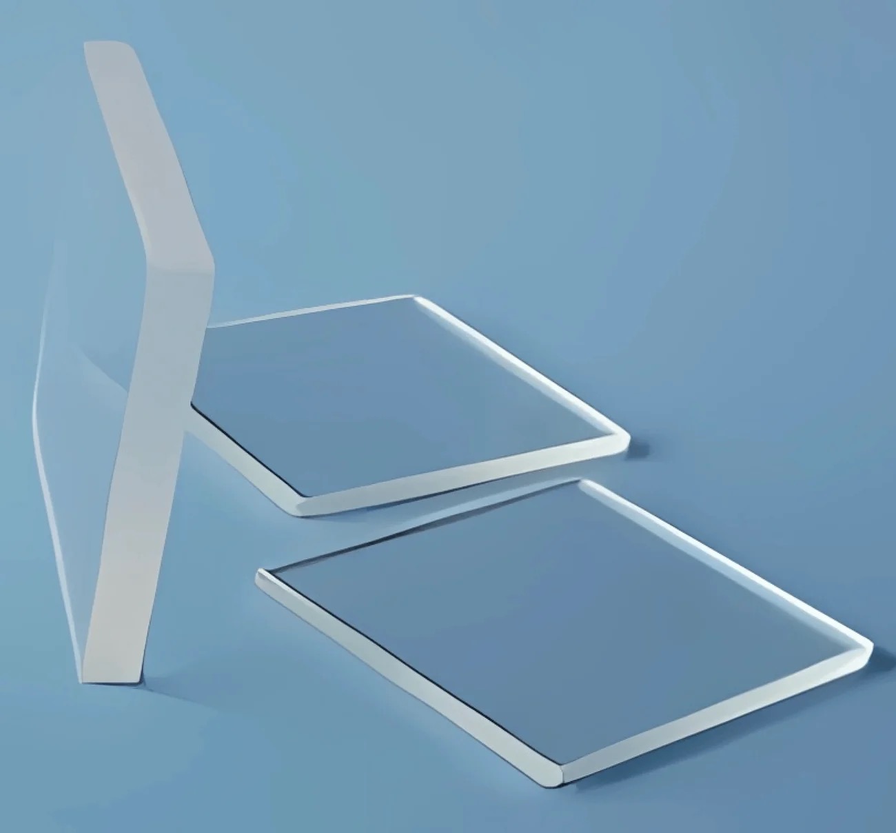
As the demand for miniaturized, high-performance electronic and photonic devices surges, the Quartz Wafer Diced Chip Synthetic Quartz Double-Side Polished Substrate emerges as a cornerstone of precision manufacturing. Crafted from ultra-pure synthetic quartz and meticulously diced into chips, this substrate combines atomic-level smoothness, thermal resilience, and dimensional accuracy to meet the rigorous demands of advanced microelectronics, MEMS, and integrated photonics. This article explores its features, applications, and why it is indispensable for next-generation technologies.
Key Features
Ultra-High Purity Synthetic Quartz
Made from 99.99% synthetic fused silica (SiO₂), ensuring minimal impurities (<1 ppm) for contamination-sensitive processes in semiconductor and photonic fabrication.Double-Side Polished Precision
Both surfaces polished to sub-5 Å (angstrom) roughness, enabling defect-free thin-film deposition, lithography, and optical coatings.Precision Dicing Technology
Laser or mechanical dicing achieves micron-level accuracy for chip dimensions, ideal for microelectronics, MEMS, and sensor arrays.Exceptional Thermal Stability
Near-zero thermal expansion (CTE: 0.55 x 10⁻⁶/°C) prevents warping during high-temperature processes like annealing or bonding.Chemical and Plasma Resistance
Withstands aggressive etchants, solvents, and plasma environments, ensuring longevity in harsh semiconductor workflows.SEMI Compliance
Meets SEMI standards for flatness, purity, and defect density, compatible with automated handling systems in cleanrooms.
Applications
Microelectronics & IC Packaging: Interposers, hermetic seals, and substrates for advanced 3D IC integration.
Photonics & Optoelectronics: Waveguides, optical modulators, and laser diodes for telecom and LiDAR systems.
MEMS & Sensors: Accelerometers, gyroscopes, and pressure sensors requiring thermal and mechanical stability.
Quantum Devices: Chips for qubit arrays and photonic circuits in quantum computing systems.
Aerospace & Defense: High-reliability components for satellite optics, IR sensors, and avionics.
Why Choose Diced Quartz Substrates?
Enhanced Yield: Ultra-smooth surfaces minimize defects in lithography and thin-film processes.
Scalability: Precision dicing supports high-volume production of miniaturized components.
Versatility: Compatible with photolithography, etching, bonding, and CVD/PVD processes.
Durability: Resists thermal shock and chemical degradation, reducing lifecycle costs.
Future-Ready: Enables innovations in AI, IoT, and quantum technologies.
Conclusion
The Quartz Wafer Diced Chip Synthetic Quartz Double-Side Polished Substrate is a vital enabler of precision in modern microelectronics and photonics. Its unmatched purity, thermal stability, and sub-micron accuracy empower engineers to push the boundaries of device miniaturization and performance. Whether for cutting-edge MEMS, quantum computing, or aerospace systems, this substrate delivers reliability and efficiency in the most demanding applications.