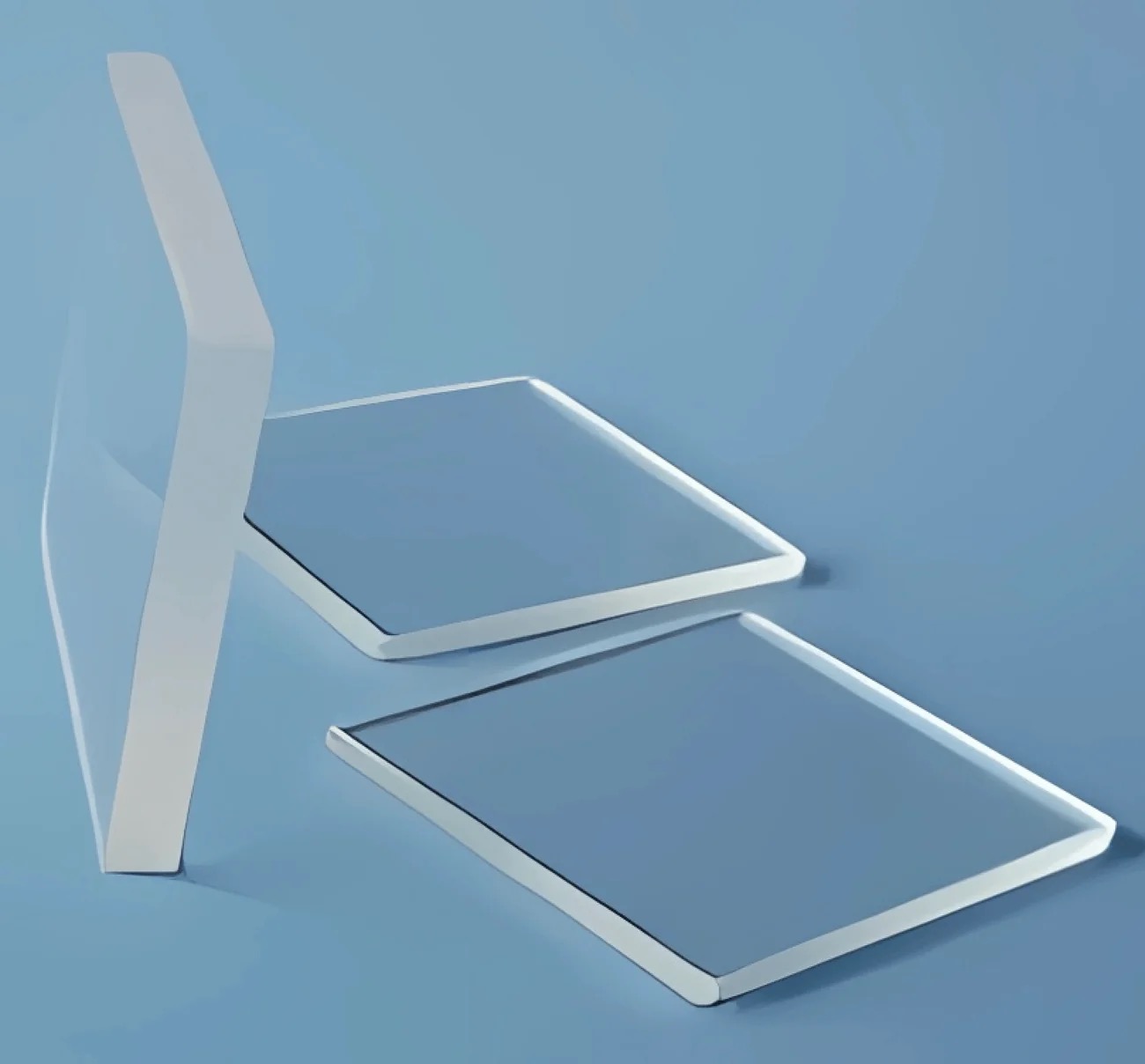
Quartz Wafer 6025 LSI Photo Mask Synthetic Quartz Substrate: Precision for Next-Gen Semiconductor Lithography
Introduction
In the race to produce smaller, faster, and more efficient semiconductor devices, the quality of photomasks directly impacts manufacturing success. The Quartz Wafer 6025 LSI Photo Mask Synthetic Quartz Substrate is a critical component designed for advanced lithography processes, particularly in large-scale integration (LSI) and extreme ultraviolet (EUV) applications. Crafted from high-purity synthetic quartz, this substrate ensures minimal defects, exceptional thermal stability, and optical precision for cutting-edge chip production. This article explores its features, applications, and why it’s indispensable for modern semiconductor fabs.
Key Features
Ultra-High Purity Synthetic Quartz
Composed of 99.99% synthetic fused silica (SiO₂), free from bubbles and inclusions, ensuring defect-free patterning for sub-5nm semiconductor nodes.Low Thermal Expansion (LTEM)
Near-zero coefficient of thermal expansion (CTE: 0.05 ppm/°C) maintains dimensional stability during high-energy EUV lithography and thermal cycling.EUV-Grade Surface Quality
Double-side polished to <0.5 nm surface roughness, critical for minimizing light scattering and achieving precise pattern transfer in EUV/DUV systems.High Optical Transparency
Superior transmittance (>90%) at 13.5 nm (EUV) and 193 nm (DUV) wavelengths, essential for high-resolution lithography.Chemical and Plasma Resistance
Withstands aggressive etchants, cleaning solvents, and plasma environments, extending photomask lifespan in repetitive fabrication cycles.Industry-Standard Dimensions
6025 specification (6-inch/150mm diameter, 6.35mm thickness) compatible with automated mask handling and inspection tools (SMIF, EUV pods).
Applications
LSI and VLSI Lithography: Photomasks for CPUs, GPUs, and memory chips in 5nm/3nm nodes.
EUV Lithography: Critical substrate for EUV mask blanks in advanced semiconductor manufacturing.
MEMS and Sensors: High-precision patterning for microelectromechanical systems.
Display Manufacturing: Masks for OLED and micro-LED display production.
Research & Development: Prototyping next-gen photonic and quantum devices.
Why Choose the 6025 Synthetic Quartz Substrate?
Yield Enhancement: Ultra-smooth surfaces reduce defects, improving lithography accuracy and chip yield.
Durability: Resists thermal warping and chemical degradation, lowering total cost of ownership (TCO).
SEMI Compliance: Meets SEMI Standard F57 for flatness, purity, and defect density.
Future-Ready: Supports emerging technologies like high-NA EUV and 3D IC packaging.
Conclusion
The Quartz Wafer 6025 LSI Photo Mask Synthetic Quartz Substrate is the backbone of precision in semiconductor lithography. Its unmatched purity, thermal stability, and EUV compatibility make it essential for producing cutting-edge chips powering AI, 5G, and IoT technologies. For fabs aiming to lead in advanced manufacturing, this substrate is a strategic investment in quality and innovation.


