Glass Wafer 4-Inch High Purity Double-Side Polished Optical Substrate: Precision for Advanced Photonics and MEMS
Introduction
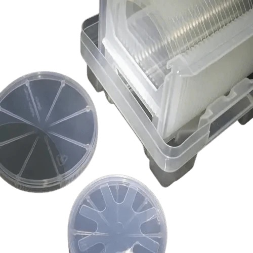
In industries where precision optics and material reliability are critical, the Glass Wafer 4-Inch High Purity Double-Side Polished Optical Substrate serves as a foundational component for cutting-edge technologies. Combining ultra-smooth surfaces, exceptional purity, and thermal resilience, this substrate is tailored for applications ranging from advanced photonics to microelectromechanical systems (MEMS). This article explores its features, uses, and advantages in modern manufacturing and research.
Key Features
Ultra-High Purity Material
Manufactured from low-alkali borosilicate or fused silica glass, ensuring minimal ionic contamination (<1 ppm) for sensitive optical and electronic processes.Double-Side Polished Surfaces
Both sides polished to a surface roughness of <5 Å (angstroms), achieving near-atomic smoothness for high-precision lithography, coatings, and bonding.Optical Clarity
High transmittance (>90%) across visible and near-UV wavelengths (350–2000 nm), ideal for lenses, filters, and optical sensors.Thermal and Chemical Stability
Withstands temperatures up to 500°C and resists acids, alkalis, and moisture, ensuring durability in harsh fabrication environments.Low Thermal Expansion
Coefficient of thermal expansion (CTE: 3.25–5.5 x 10⁻⁶/°C) minimizes dimensional shifts during thermal cycling, critical for MEMS and semiconductor processes.Customizable Dimensions
Standard 4-inch (100mm) diameter with thickness options from 0.1mm to 2mm, adaptable to prototyping or high-volume production needs.
Applications
Photonics & Optics: Substrates for waveguides, laser optics, anti-reflective coatings, and optical sensors.
MEMS & Sensors: Base material for pressure sensors, accelerometers, and biochips requiring thermal stability.
Semiconductor Packaging: Interposers, hermetic seals, and carriers for advanced IC integration.
Display Technology: Glass carriers for OLED and micro-LED manufacturing processes.
Biotechnology: Microfluidic devices and lab-on-a-chip platforms for medical diagnostics.
Why Choose This Glass Substrate?
Enhanced Precision: Ultra-smooth surfaces reduce defects in thin-film deposition and etching, improving yield.
Versatility: Compatible with photolithography, wet/dry etching, anodic bonding, and laser machining.
Cost Efficiency: Offers optical performance comparable to quartz at a lower cost.
Industry Compliance: Meets SEMI, ISO 9001, and MIL-STD standards for quality and traceability.
Conclusion
The 4-inch high-purity double-side polished glass wafer is a vital enabler of innovation in optics, MEMS, and semiconductor industries. Its exceptional smoothness, thermal resilience, and adaptability make it indispensable for developing next-generation technologies, from augmented reality displays to precision biomedical devices. For engineers and researchers prioritizing performance and reliability, this substrate delivers unmatched value.