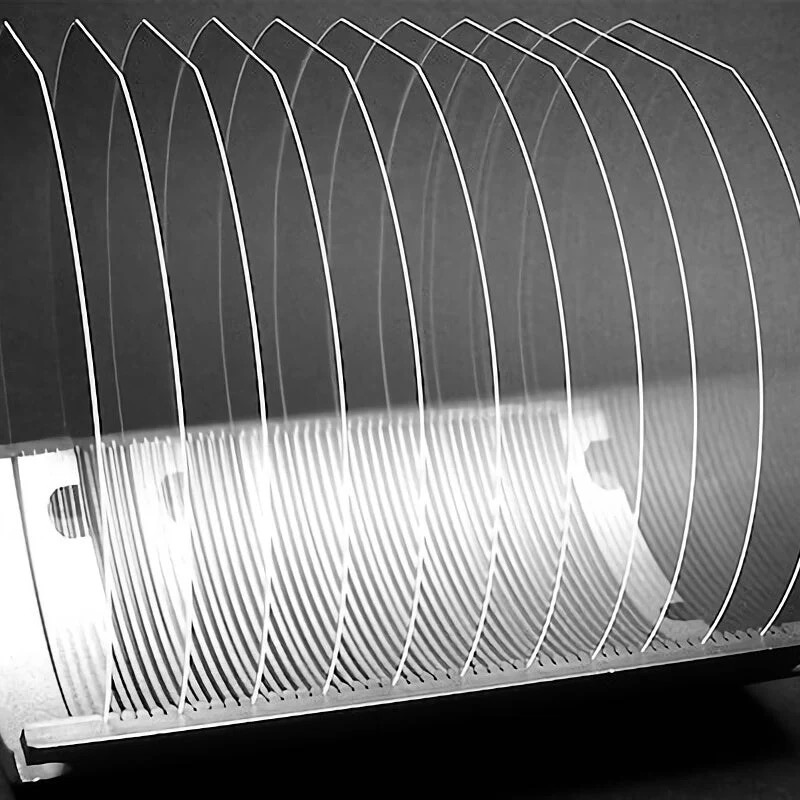
Glass Wafer 6-Inch B270 Double-Side Polished Substrate: Precision for Optics and MEMS Applications
Introduction
In industries where optical precision and material versatility are paramount, the Glass Wafer 6-Inch B270 Double-Side Polished Substrate emerges as a critical component. Crafted from borosilicate glass (B270), this substrate combines superior optical performance, chemical resistance, and mechanical durability, making it a go-to solution for advanced photonics, semiconductor packaging, and microelectromechanical systems (MEMS). This article explores its features, applications, and why it stands out in high-tech manufacturing.
Key Features of the B270 Glass Wafer
Optical-Grade Clarity
B270 borosilicate glass offers high transmittance (>90%) across visible and near-UV spectra (350–2000 nm), perfect for lenses, filters, and optical coatings.Double-Side Polished Precision
Both surfaces are polished to a roughness of <5 Å (angstroms), ensuring ultra-smoothness for nanoscale lithography and thin-film deposition.Thermal and Chemical Resilience
Withstands temperatures up to 450°C and resists acids, alkalis, and moisture, ideal for harsh fabrication environments.Low Thermal Expansion
Coefficient of thermal expansion (CTE: 3.25 x 10⁻⁶/°C) ensures stability during thermal cycling, critical for MEMS and semiconductor processes.Customizable Dimensions
Standard 6-inch (150mm) diameter with thickness options from 0.1mm to 3mm, tailored for prototyping or mass production.Cost-Effective Alternative
Provides similar optical performance to fused silica at a lower cost, ideal for budget-sensitive projects.
Primary Applications
Photonics & Optics: Substrates for lenses, beam splitters, anti-reflective coatings, and optical sensors.
MEMS & Sensors: Base material for pressure sensors, accelerometers, and biochips requiring thermal stability.
Semiconductor Packaging: Interposers and hermetic seals for advanced IC packaging.
Display Technology: Glass carriers for OLED and micro-LED manufacturing.
Biotechnology: Microfluidic chips and lab-on-a-wafer devices for medical diagnostics.
Why Choose B270 Glass Wafers?
Enhanced Precision: Ultra-smooth surfaces minimize defects in lithography and thin-film processes.
Versatility: Compatible with wet/dry etching, laser machining, and anodic bonding.
Durability: Resists delamination and chemical degradation, extending product lifespan.
Industry Compliance: Meets ISO 9001 and SEMI standards for quality and traceability.
Conclusion
The 6-inch B270 double-side polished glass wafer bridges the gap between performance and affordability, offering a robust solution for optics, MEMS, and semiconductor industries. Its optical clarity, thermal resilience, and adaptability make it indispensable for innovators developing next-generation technologies, from augmented reality displays to precision biomedical devices.


