Quartz Wafer 12-Inch High-Purity Double-Side Polished Substrate: Precision for Next-Gen Technologies
Introduction
As industries push the limits of miniaturization and performance, the demand for larger, ultra-precise substrates grows exponentially. The Quartz Wafer 12-Inch High-Purity Double-Side Polished Substrate meets this challenge head-on, offering unparalleled material quality and surface precision for semiconductor fabrication, quantum computing, and high-power laser systems. This article explores its features, applications, and why it’s critical for next-generation technologies.
Key Features of the 12-Inch Quartz Wafer
Ultra-High Purity (S2/Synthetic Fused Silica)
Composed of 99.999% synthetic fused quartz (SiO₂), ensuring minimal impurities for critical processes like EUV lithography and high-energy laser optics.Double-Side Polished Perfection
Both surfaces achieve sub-5 Å (angstrom) roughness, eliminating defects and enabling nanoscale patterning for advanced semiconductor nodes and optical coatings.Extreme Thermal and Chemical Resistance
Withstands temperatures up to 1,200°C and resists plasma etching, acids, and alkalis, ideal for harsh semiconductor and aerospace environments.Near-Zero Thermal Expansion
Exceptionally low coefficient of thermal expansion (CTE < 0.55 x 10⁻⁶/°C) ensures dimensional stability during rapid thermal cycling.Broad Optical Transparency
High transmittance across UV (190 nm) to IR (2,500 nm) wavelengths, critical for deep-UV lithography, laser optics, and IR sensor systems.Large-Format Compatibility
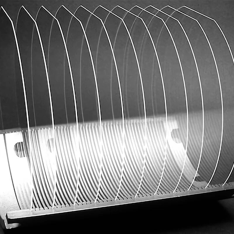
12-inch (300mm) diameter supports high-throughput manufacturing of advanced semiconductors, photonic circuits, and MEMS devices.
Primary Applications
Advanced Semiconductor Manufacturing: EUV lithography mask substrates for sub-5nm chip nodes.
Photonics and Quantum Computing: Base material for integrated photonic circuits and qubit arrays.
High-Power Laser Systems: Optical windows, lenses, and beam delivery components resistant to laser-induced damage.
Aerospace & Defense: IR-transparent radomes, sensor protection, and satellite optics.
MEMS and Sensors: Precision substrates for microelectromechanical systems requiring thermal stability.
Why Choose a 12-Inch Quartz Substrate?
Scalability: Large 12-inch format aligns with 300mm wafer fabs, reducing costs in high-volume production.
Yield Optimization: Ultra-smooth surfaces minimize defects in thin-film deposition and etching processes.
Future-Proofing: Supports emerging technologies like quantum dots, photonic ICs, and EUV lithography.
Regulatory Compliance: Meets SEMI, MIL-STD, and ISO 9001 standards for traceability and quality control.
Conclusion
The 12-inch high-purity double-side polished quartz wafer is a cornerstone of innovation in semiconductor, photonics, and defense industries. Its exceptional purity, thermal resilience, and optical precision make it indispensable for next-gen technologies demanding larger formats and atomic-level accuracy. Whether for EUV lithography, quantum devices, or aerospace optics, this substrate delivers unmatched performance in the most demanding environments.