Quartz Wafer (S2) 6-Inch High-Purity Double-Side Polished Substrate: Precision for Advanced Applications
Introduction
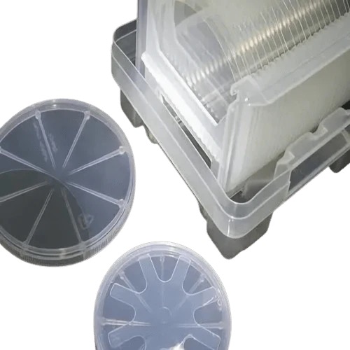
In high-tech industries where precision and material purity are non-negotiable, the Quartz Wafer (S2) 6-Inch Double-Side Polished Substrate stands out as a cornerstone for cutting-edge applications. Made from synthetic fused quartz with exceptional purity (S2 grade), this substrate is designed for demanding environments, including semiconductor lithography, MEMS fabrication, and laser optics. This article delves into its specifications, benefits, and why it’s a top choice for engineers and researchers.
Key Features of the S2 Quartz Wafer
Ultra-High Purity (S2 Grade)
Composed of 99.99% synthetic fused silica (SiO₂), minimizing impurities for critical processes like UV photolithography and laser optics.Double-Side Polished Precision
Both surfaces are polished to a roughness of <5 Å (angstroms), ensuring minimal light scattering and optimal flatness for nanoscale fabrication.Thermal and Chemical Resilience
Withstands extreme temperatures (up to 1,100°C) and resists acids, alkalis, and plasma etching, making it ideal for harsh semiconductor environments.Low Thermal Expansion
Near-zero coefficient of thermal expansion (CTE) ensures dimensional stability under rapid temperature changes.Optical Clarity
High transmittance across UV to IR spectra (190 nm to 2,500 nm), perfect for optical windows, lenses, and laser systems.Standard and Custom Sizes
Available in 6-inch diameter with thicknesses from 0.5mm to 3mm, supporting both R&D prototyping and mass production.
Primary Applications
Semiconductor Lithography: Mask substrates for EUV and DUV photolithography processes.
MEMS and Sensors: Base material for microelectromechanical systems requiring thermal stability.
Laser and Optics: Windows, lenses, and beam splitters in high-power laser systems.
Quantum Technology: Substrates for qubit arrays and photonic circuits.
Aerospace and Defense: Radomes, IR optics, and sensor protection in extreme conditions.
Why Choose S2-Grade Quartz Wafers?
Yield Enhancement: Ultra-smooth surfaces reduce defects in thin-film deposition and etching.
Durability: Long lifespan under aggressive chemical and thermal processes lowers replacement costs.
Versatility: Compatible with photolithography, etching, CVD, and PVD processes.
Industry Compliance: Meets SEMI, MIL-STD, and ISO cleanroom standards for traceability and quality assurance.
Conclusion
The Quartz Wafer (S2) 6-inch double-side polished substrate is an indispensable material for industries pushing the boundaries of precision engineering. Its unmatched purity, thermal resilience, and optical performance make it a trusted solution for semiconductor fabrication, advanced optics, and next-generation technologies like quantum computing.