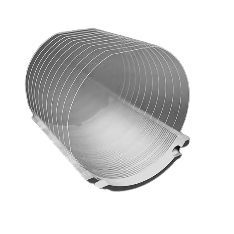
Silicon Wafer 4-Inch N-Type 0.01~0.09Ω·cm with 300nm Oxide Layer: Engineered for High-Performance Semiconductor Devices
Introduction
Silicon wafers remain the backbone of modern electronics, and the 4-inch N-Type silicon wafer with 0.01~0.09Ω·cm resistivity and a 300nm oxide layer exemplifies precision engineering for cutting-edge applications. Tailored for high conductivity, thermal stability, and surface passivation, this substrate is critical for power devices, sensors, and integrated circuits. This article explores its specifications, advantages, and key use cases.
What Makes This Silicon Wafer Unique?
This substrate combines N-Type doping (typically phosphorus or arsenic) with ultra-low resistivity (0.01~0.09Ω·cm) and a uniform 300nm oxide layer. The oxide layer, grown via thermal oxidation or CVD, serves as an insulator, protective barrier, or dielectric in device fabrication. Its 4-inch diameter ensures compatibility with standard semiconductor tools for prototyping and production.
Key Specifications & Features
Electrical Performance
Low Resistivity (0.01~0.09Ω·cm): Enables efficient current flow for high-power and high-frequency devices.
N-Type Doping: Provides electron-rich conductivity, ideal for MOSFETs, diodes, and solar cells.
Oxide Layer (300nm)
Acts as a gate dielectric, passivation layer, or mask for etching/doping processes.
Enhances device reliability by preventing contamination and leakage currents.
Surface Quality
Double-side polished for minimal surface roughness (<0.5nm), critical for lithography accuracy.
Thermal & Mechanical Stability
Withstands high-temperature processes (e.g., annealing, oxidation) without warping.
Applications of 4-Inch N-Type Silicon Wafers with Oxide Layers
Power Electronics
Fabrication of IGBTs, thyristors, and power MOSFETs requiring low-resistance substrates.
MEMS & Sensors
Base material for pressure sensors, accelerometers, and microactuators.
Integrated Circuits (ICs)
CMOS and analog/digital ICs leveraging the oxide layer for gate insulation.
Optoelectronics
Photodetectors and LED structures where controlled doping and surface passivation are critical.
Research & Prototyping
Cost-effective substrate for testing novel semiconductor materials or processes.
Why Choose This Silicon Wafer?
Precision Doping: Ensures consistent electrical properties across the wafer.
Scalability: 4-inch size aligns with industry-standard fabrication tools.
Versatility: Oxide layer supports diverse device architectures (e.g., SOI, FinFET).
Cost Efficiency: Reduces defects and rework in high-volume manufacturing.
FAQ Section
Q: What is the role of the 300nm oxide layer?
A: It provides electrical insulation, surface passivation, and serves as a hard mask during etching or implantation.
Q: Can the resistivity be customized within the 0.01~0.09Ω·cm range?
A: Yes, resistivity can be tailored during doping to meet specific device requirements.
Q: Are these wafers suitable for high-temperature processes?
A: Absolutely—silicon’s thermal stability makes it ideal for processes like diffusion and oxidation.
Q: Is the oxide layer grown via thermal oxidation or CVD?
A: Both methods are available; thermal oxidation offers superior purity, while CVD allows faster deposition.
Conclusion
The 4-inch N-Type silicon wafer with 0.01~0.09Ω·cm resistivity and a 300nm oxide layer is a cornerstone of advanced semiconductor innovation. Its blend of low resistance, robust oxide functionality, and industry-standard sizing empowers engineers to push the limits of power efficiency, miniaturization, and device reliability. Whether for prototyping next-gen electronics or scaling production, this substrate delivers unmatched performance and versatility.
Elevate your semiconductor projects with precision-engineered silicon wafers today!


