Quartz Wafer 4-Inch Double Side Polished Synthetic Substrate: Precision for Advanced Applications
Introduction
Quartz wafers are indispensable in industries requiring ultra-pure, thermally stable, and optically transparent materials. The 4-inch double side polished synthetic quartz substrate stands out for its exceptional surface flatness and chemical resistance, making it a cornerstone for cutting-edge technologies. This article delves into its properties, applications, and why it’s a top choice for high-precision manufacturing and research.
What is a Double Side Polished (DSP) Synthetic Quartz Wafer?
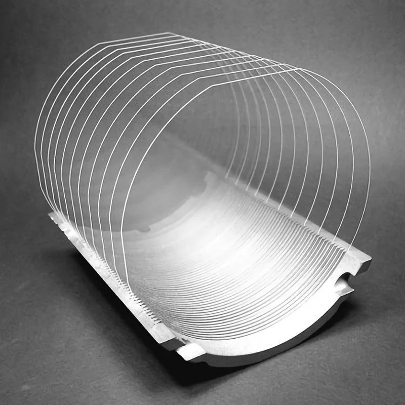
A synthetic quartz wafer is a high-purity, lab-grown crystal substrate designed for demanding technical applications. The 4-inch double side polished variant undergoes rigorous polishing on both surfaces to achieve near-perfect flatness (often with surface roughness <1 nm), ensuring minimal light scattering and optimal performance in optical and electronic systems.
Key Features of 4-Inch DSP Synthetic Quartz Wafers
Ultra-Smooth Surfaces
Double side polishing eliminates defects and ensures uniformity for nanoscale processes.
High Thermal Stability
Withstands extreme temperatures (up to 1,000°C) without warping, ideal for semiconductor fabrication.
Optical Clarity
High transparency across UV to IR spectra, critical for photolithography and optical devices.
Chemical Inertness
Resists acids, alkalis, and plasma etching, ensuring longevity in harsh environments.
Standardized Dimensions
4-inch (100mm) diameter aligns with industry equipment for seamless integration.
Applications of Double Side Polished Quartz Wafers
Semiconductor Manufacturing
Used as photomask substrates in EUV and DUV lithography for chip patterning.
Optoelectronics
Base material for optical filters, lenses, and laser components requiring minimal surface distortion.
MEMS & Sensors
Provides a stable platform for fabricating pressure sensors, accelerometers, and microfluidic devices.
Research & Metrology
Calibration standards for AFM, SEM, and other high-resolution imaging tools.
Quantum Technologies
Substrates for quantum dot arrays and photonic circuits due to low thermal expansion.
Why Choose 4-Inch DSP Synthetic Quartz Wafers?
Precision: Enables sub-nanometer accuracy in lithography and thin-film deposition.
Durability: Long-lasting performance in aggressive chemical or thermal processes.
Versatility: Compatible with semiconductors, optics, and emerging fields like quantum computing.
Cost Efficiency: Reduces defects and rework in high-value production lines.
FAQ Section
Q: How does synthetic quartz differ from natural quartz?
A: Synthetic quartz offers higher purity, fewer inclusions, and tailored properties for technical applications.
Q: Can DSP quartz wafers be customized for thickness or coatings?
A: Yes, they are often tailored in thickness (e.g., 500µm to 1mm) and can include anti-reflective or conductive coatings.
Q: Are these wafers reusable after processing?
A: Depending on the application, they can be cleaned and reused multiple times, enhancing cost-effectiveness.
Conclusion
The 4-inch double side polished synthetic quartz wafer is a critical enabler of innovation in semiconductors, optics, and advanced sensing technologies. Its unparalleled surface quality, thermal resilience, and chemical inertness make it a preferred substrate for industries pushing the boundaries of precision and performance. By integrating these wafers into your workflows, you ensure reliability, efficiency, and scalability in next-generation device manufacturing.
Upgrade your processes with precision-engineered quartz substrates today!