Introduction
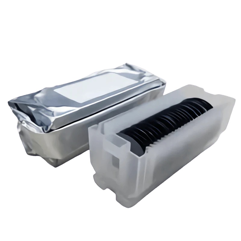
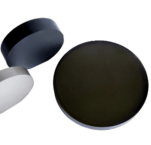
2-inch silicon wafers are compact yet powerful substrates widely used in specialized semiconductor research, prototyping, and microfabrication. This article focuses on P-type (100/111) silicon waferswith single/double-side polishing, highlighting their structural properties, applications, and advantages in advancing technologies such as microelectromechanical systems (MEMS), sensors, and optoelectronics.
Key Features
P-Type Doping
Doped with boron to create "hole" majority carriers, enabling stable performance in power devices, radiation detectors, and sensors.
Offers predictable electrical behavior for applications requiring controlled charge transport.
Crystal Orientations: (100) vs. (111)
(100) Orientation:
Preferred for integrated circuits (ICs) and CMOS processes due to uniform etching and compatibility with epitaxial growth.
Ideal for photolithography and high-yield device fabrication.
(111) Orientation:
Excels in MEMS and sensor applications due to anisotropic etching properties, enabling precise geometric structures.
Used in piezoresistive devices and optical components.
Single/Double-Side Polishing
Single-Side Polished (SSP):
Cost-effective for applications requiring one active surface (e.g., basic ICs, solar cells).
Reduces material costs while maintaining functional performance.
Double-Side Polished (DSP):
Delivers ultra-smooth surfaces (≤1nm roughness) on both sides, critical for optical devices, MEMS mirrors, and dual-sided processing.
Ensures parallelism and minimal light scattering in photonic applications.
High-Quality Material
Low defect density and high purity for reliable performance in high-frequency and high-voltage environments.
Compatible with thermal oxidation, thin-film deposition, and etching processes.
Advantages
Compact Size: Cost-effective for niche applications and compatible with legacy 2-inch fabrication tools.
Versatility: (100) orientation suits mainstream ICs, while (111) excels in MEMS and specialized sensors.
Surface Quality: Polishing minimizes defects, enhancing device reliability and manufacturing yield.
Scalability: Bridges the gap between R&D and low-volume production for emerging technologies.
Choosing the Right Configuration
Select Orientation Based on Use:
(100): Choose for ICs, epitaxial layers, or photovoltaics.
(111): Opt for MEMS, anisotropic etching, or piezoresistive sensors.
Polishing Needs:
Use DSP for optical clarity or dual-surface MEMS designs.
SSP suffices for single-layer devices or budget-constrained projects.
Conclusion
2-inch P-type (100/111) single/double-side polished silicon wafers are indispensable for innovators in semiconductor research and microfabrication. Their adaptability across crystal orientations and polishing configurations makes them ideal for MEMS, sensors, and optoelectronic systems. By aligning wafer specifications with application demands, engineers and researchers can achieve precision and efficiency in cutting-edge technologies.