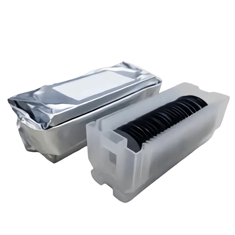
Introduction to 3-Inch N-Type Silicon Wafers
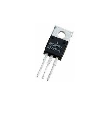
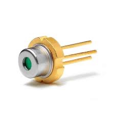
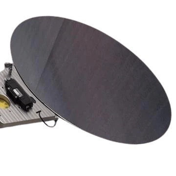
N-Type silicon wafers are fundamental to modern electronics, offering superior electron mobility for high-speed and high-frequency applications. This article examines 3-inch N-Type (100/111) silicon wafers with single/double-side polishing, detailing their structural advantages, key applications, and role in advancing semiconductor technologies such as RF devices, photonics, and MEMS.
Key Features of the Wafer
N-Type Doping with (100/111) Orientation
N-Type Conductivity: Doped with phosphorus or arsenic to provide free electrons, enabling high-speed electron conduction for transistors, diodes, and RF components.
Crystal Orientation Flexibility:
(100) Orientation: Widely used in CMOS fabrication, epitaxial growth, and integrated circuits due to uniform etching and compatibility with standard processes.
(111) Orientation: Favored for MEMS, piezoelectric sensors, and optoelectronic devices due to anisotropic etching behavior and strong interfacial properties.
Single/Double-Side Polishing
Single-Side Polished (SSP): Cost-effective for applications requiring only one active surface (e.g., solar cells, basic ICs).
Double-Side Polished (DSP): Essential for optical devices, advanced sensors, and MEMS where ultra-smooth surfaces (≤0.5nm roughness) and parallelism are critical.
High Material Quality
Low defect density and high purity ensure minimal carrier recombination, enhancing device efficiency.
Compatible with thermal oxidation, CVD/PVD deposition, and photolithography for complex device architectures.
Research & Prototyping: 3-inch size offers a practical balance between cost and functionality for academic labs.
Advantages of 3-Inch N-Type Wafers
Enhanced Electron Mobility: N-type doping ensures faster electron transport, critical for high-speed and low-power devices.
Surface Precision: Polishing minimizes defects and roughness, improving yield in photolithography and thin-film processes.
Orientation Versatility: (100) for mainstream ICs; (111) for MEMS and specialized optoelectronics.
Scalability: Compatible with legacy 3-inch equipment, reducing transition costs for labs and small-scale fabs.
Selecting the Optimal Configuration
Match Orientation to Application:
(100): Choose for CMOS, logic circuits, or epitaxial growth.
(111): Opt for MEMS, sensors, or devices requiring precise anisotropic etching.
Polishing Requirements:
Use DSP for optical applications (e.g., waveguides) or dual-sided MEMS structures.
SSP suffices for single-layer devices or cost-sensitive projects.
Doping Concentration: Ensure phosphorus/arsenic levels align with target resistivity (e.g., low resistivity for high-current devices).
Conclusion
3-inch N-Type (100/111) single/double-side polished silicon wafers are pivotal for next-generation semiconductor innovation. Their high electron mobility, crystal orientation flexibility, and superior surface quality make them indispensable for RF systems, optoelectronics, MEMS, and power devices. By tailoring wafer specifications to application needs, engineers and researchers can achieve optimal performance and efficiency in cutting-edge technologies.
