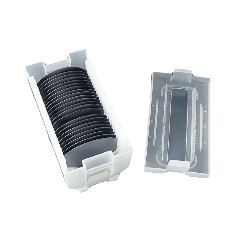
Introduction to 3-Inch P-Type Silicon Wafers
3-inch silicon wafers are a critical substrate in semiconductor manufacturing, offering a balance between compact size and sufficient surface area for prototyping and specialized device fabrication. This article focuses on P-type (100/111) silicon wafers with single/double-side polishing, highlighting their structural advantages, applications, and suitability for high-precision technologies such as MEMS, optoelectronics, and integrated circuits.
Key Features of the Wafer
P-Type Doping (100/111) Orientation
P-Type Conductivity: Doped with boron to create hole-dominated conduction, ideal for power devices, sensors, and radiation-hardened applications.
Crystal Orientation Options:
(100) Orientation: Preferred for CMOS fabrication, epitaxial growth, and photolithography due to uniform etching properties.
(111) Orientation: Valued for MEMS, piezoresistive sensors, and optoelectronic devices, leveraging its anisotropic etching behavior.
Single/Double-Side Polishing
Single-Side Polished (SSP): Cost-effective for applications requiring only one active surface (e.g., solar cells, simple ICs).
Double-Side Polished (DSP): Essential for optical devices, MEMS, and advanced sensors where parallelism and surface smoothness (<1nm roughness) are critical.
High-Quality Substrate
Low defect density and high purity ensure reliable performance in high-frequency and high-voltage applications.
Compatible with thermal oxidation, thin-film deposition, and photolithography processes.
Advantages of 3-Inch P-Type Wafers
Size Flexibility: Larger than 2-inch wafers for expanded design space, yet compact enough for cost-sensitive projects.
Surface Quality: Polishing minimizes defects, enhancing device yield and performance.
Orientation Versatility: (100) for standard ICs; (111) for MEMS and specialized etching.
Compatibility: Works with legacy 3-inch fabrication equipment, reducing upgrade costs.
Choosing the Right Configuration
Opt for DSP for Optical/MEMS: Double-side polishing is critical for applications requiring light transmission or dual-surface processing.
Select Orientation Based on Use Case:
(100) for epitaxial layers, CMOS, and photovoltaics.
(111) for MEMS, pressure sensors, and anisotropic etching.
Verify Doping Levels: Ensure boron concentration aligns with target resistivity (e.g., moderate doping for sensors, heavy doping for power devices).
Conclusion
3-inch P-type (100/111) single/double-side polished silicon wafers are indispensable for cutting-edge semiconductor and microsystems engineering. Their versatility in crystal orientation, surface finish, and size makes them ideal for MEMS, optoelectronics, and power electronics. By aligning wafer specifications with application needs, researchers and manufacturers can optimize performance and cost-efficiency.