Introduction to High-Resistivity Float-Zone (FZ) Silicon Wafers
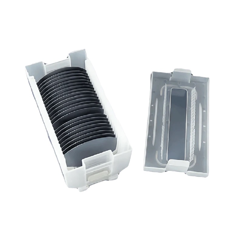
Float-Zone (FZ) silicon wafers are renowned for their ultra-high purity and minimal crystal defects, making them essential for high-frequency, high-power, and precision optical applications. This article examines 2-inch FZ silicon wafers with P/N type doping, >1000Ω·cm resistivity, (100/111) crystal orientations, and single/double-sided polishing, highlighting their role in advanced semiconductor and optoelectronic systems.
Key Features of the Wafer
Float-Zone (FZ) Growth Method
Produces ultra-pure silicon with negligible oxygen and carbon contamination.
Ideal for high-resistivity (>1000Ω·cm) applications requiring minimal signal loss.
P/N Type Doping (100/111) Orientation
P-Type (100/111): Doped with boron for hole conduction; used in radiation detectors and high-voltage devices.
N-Type (100/111): Doped with phosphorus/arsenic for electron conduction; suited for RF transistors and photodiodes.
(100) Orientation: Preferred for epitaxial growth and MOSFET fabrication.
(111) Orientation: Favored for MEMS, sensors, and optoelectronic devices due to anisotropic etching properties.
Ultra-High Resistivity (>1000Ω·cm)
Minimizes parasitic capacitance and signal attenuation, critical for RF/microwave circuits and quantum computing components.
Reduces leakage currents in high-voltage power devices and photonic sensors.
Single/Double-Sided Polishing
Single-Sided: Cost-effective for applications requiring only one active surface (e.g., solar cells).
Double-Sided: Essential for MEMS, optical windows, and devices requiring dual-surface processing.
Advantages of 2-Inch FZ Wafers
Ultra-Low Defect Density: Ensures consistent performance in sensitive applications.
Thermal Stability: Maintains integrity under high-power operation.
Versatile Orientation Options: (100) for epitaxy and ICs; (111) for MEMS and optics.
Customizable Polishing: Double-sided polishing enhances optical clarity and parallelism.
Choosing the Right Wafer
Resistivity Needs: Use >1000Ω·cm substrates for RF or high-voltage devices to minimize losses.
Crystal Orientation: Select (100) for CMOS or epitaxial layers; (111) for anisotropic etching in MEMS.
Polishing Type: Opt for double-sided polishing for optical or dual-sided fabrication processes.
Conclusion
2-inch FZ P/N type (100/111) silicon wafers with >1000Ω·cm resistivity and single/double-sided polishing are indispensable for cutting-edge technologies demanding ultra-high purity and precision. Their unique properties cater to RF systems, photonics, and power devices, offering unmatched performance in high-stakes environments. Collaborate with specialized suppliers to tailor specifications for your application’s exact requirements.


