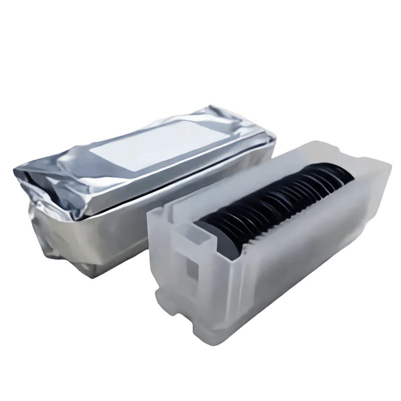
Introduction to High-Conductivity 2-Inch Silicon Wafers
Silicon wafers with ultra-low resistivity and precise crystal orientations are critical for high-performance semiconductor devices. The 2-inch P/N Type (100) silicon wafer, featuring an ultra-low resistivity range of 0.001–0.009Ω and a functional oxide layer, is engineered for demanding applications in power electronics, radio frequency (RF) components, and advanced integrated circuits. This article explores its unique properties, applications, and benefits.
Key Features of the Silicon Wafer
P/N Type (100) Crystal Orientation
The (100) crystal orientation is widely used for its compatibility with epitaxial growth, CMOS fabrication, and anisotropic etching processes.
P-Type (100): Doped with boron for hole conduction, ideal for power devices and high-current applications.
N-Type (100): Doped with phosphorus or arsenic for electron conduction, preferred for high-frequency transistors and RF amplifiers.
Ultra-Low Resistivity (0.001–0.009Ω)
This extremely low resistivity indicates heavy doping, enabling minimal energy loss and high current-carrying capacity.
Ideal for power semiconductors (e.g., IGBTs, MOSFETs) and high-efficiency solar cellswhere conductivity is paramount.
Oxide Layer (SiO₂)
A thermally grown or deposited silicon dioxide layer provides electrical insulation, surface passivation, and a stable interface for photolithography.
Critical for gate oxides in transistors, MEMS fabrication, and protective coatings in harsh environments.
Advantages of 2-Inch Wafers with Ultra-Low Resistivity
Superior Electrical Performance: Ultra-low resistivity reduces heat generation and energy waste in high-power applications.
Precision Doping Control: Ensures consistent conductivity for reliable device performance.
Compact and Cost-Effective: Smaller wafer size reduces material costs for prototyping and specialized production.
Oxide Layer Versatility: Supports both insulation and patterning processes in semiconductor manufacturing.
Choosing the Right Wafer
Match Resistivity to Current Needs: Use 0.001–0.009Ω wafers for applications requiring minimal resistance (e.g., power modules).
Crystal Orientation Matters: The (100) orientation ensures compatibility with standard fabrication techniques like dry etching and epitaxy.
Verify Oxide Thickness: Ensure the oxide layer meets requirements for insulation, masking, or surface passivation.
Conclusion
The 2-inch P/N Type (100) silicon wafer with ultra-low 0.001–0.009Ω resistivity and an oxide layer is a cornerstone for cutting-edge semiconductor technologies. Its exceptional conductivity, paired with the versatility of the (100) orientation, makes it indispensable for power electronics, RF systems, and advanced ICs. For tailored solutions, collaborate with suppliers to align wafer specifications with your project’s technical demands.