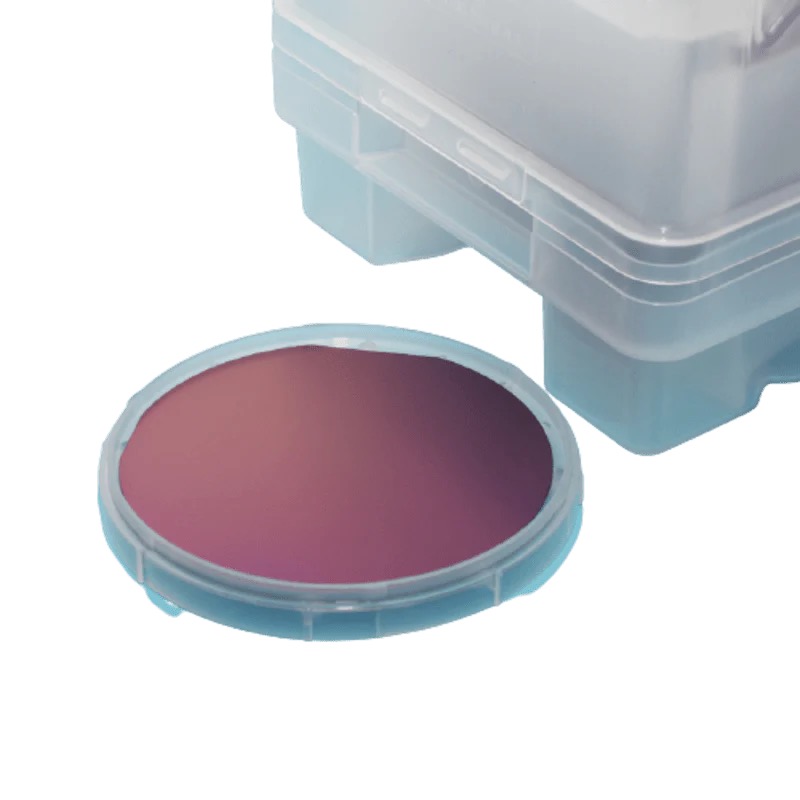
Introduction to 2-Inch Silicon Wafers
Silicon wafers are the backbone of modern semiconductor technology. A 2-inch silicon wafer, though smaller compared to industrial standards, is widely used in research, prototyping, and specialized applications due to its cost-effectiveness and compatibility with smaller fabrication tools. This article delves into the features and applications of 2-inch P/N type silicon wafers with 1–10Ω resistivity and an oxide layer.
Key Features of the Silicon Wafer
P/N Type Conductivity
P-Type: Doped with elements like boron to create "holes" (positive charge carriers), ideal for applications requiring hole-dominated conduction.
N-Type: Doped with phosphorus or arsenic to provide free electrons (negative charge carriers), preferred for high-speed electronic devices.
1–10Ω Resistivity Range
This moderate resistivity balances conductivity and power efficiency, making it suitable for analog circuits, sensors, and MEMS (Micro-Electro-Mechanical Systems).
Oxide Layer (SiO₂)
The thermally grown or deposited oxide layer acts as an insulator, protects the silicon surface, and enables critical processes like photolithography and etching in IC fabrication.
Advantages of 2-Inch Wafers
Lower material waste for small-batch production.
Compatible with legacy equipment in academic labs.
Oxide layer enhances device reliability and performance.
Choosing the Right Wafer
Select P/N type based on device requirements (e.g., N-type for high-frequency circuits). Ensure resistivity matches your application’s current handling needs. Verify oxide thickness for insulation or masking purposes.
Conclusion
2-inch P/N type silicon wafers with 1–10Ω resistivity and oxide layers are versatile substrates for semiconductor innovation. Their adaptability makes them indispensable in research and niche manufacturing. For tailored solutions, consult suppliers to align specifications with project goals.