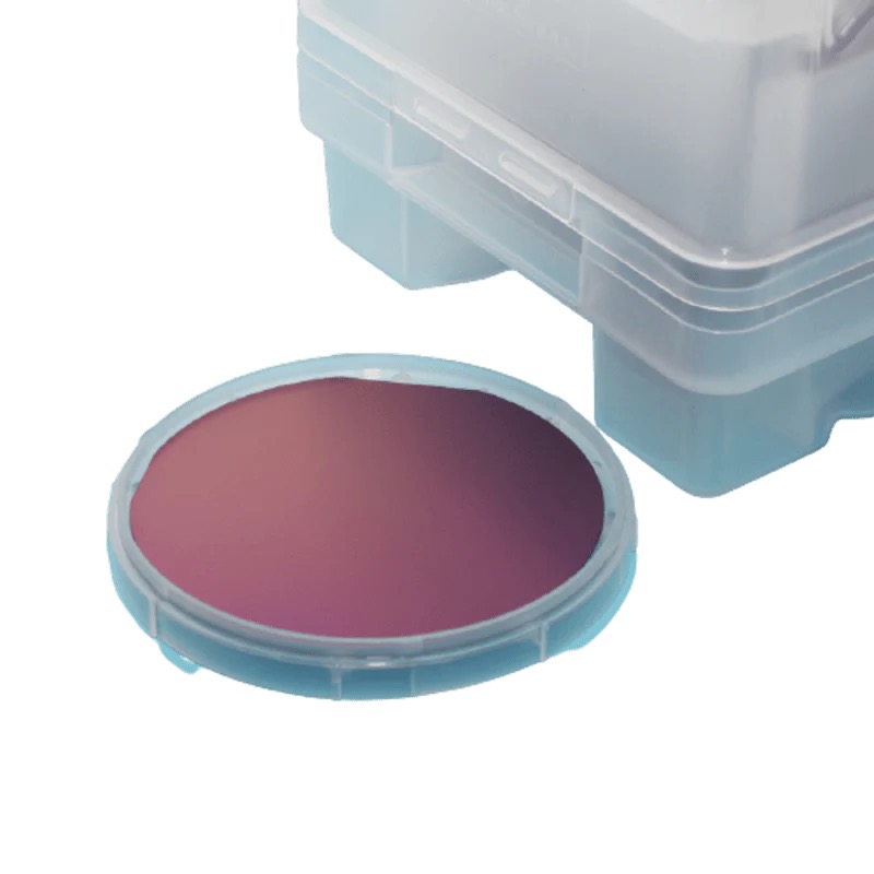
High-performance 2-inch P-type silicon wafers (10~20Ω·cm) with integrated oxide layers
Designed for power electronics, sensors, and integrated circuits, our 2-inch P-type silicon wafers feature precise resistivity (10 to 20Ω·cm) and high-quality oxide layers for high-stability, high-reliability semiconductor manufacturing needs. Through the boron doping process and thermal oxidation technology, the wafer performs well in high temperature and high pressure environments, meeting R&D and industrial application scenarios.
Core advantages and technical parameters
Medium resistivity range: 10~20Ω·cm resistivity, balance conductivity and thermal management performance, suitable for medium and high power devices and analog circuit design.
P-type boron doping: optimized hole carrier mobility, suitable for power MOSFET, IGBT, diode and other device manufacturing.
Oxide layer function:The heat grown SiO₂ layer provides surface passivation and insulation protection to reduce leakage current.
Compatible with photolithography, etching and thin film deposition processes, support complex device structure manufacturing.
2-inch standard size: Suitable for laboratory equipment and small-batch production lines, reducing prototype development costs and improving R&D efficiency.
Strict process control: to ensure doping uniformity, oxide thickness consistency and surface flatness (Ra < 0.5nm).
High environmental adaptability: Supports a wide temperature range from -50°C to 300°C, suitable for harsh scenarios such as automotive electronics and industrial power supplies.
Flexibility and compatibility: The 2-inch size is compatible with most R&D equipment, enabling rapid prototyping and small-scale production.