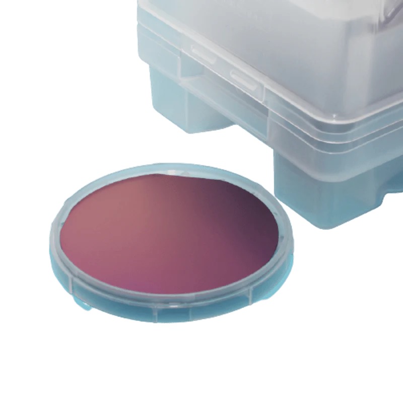
3-Inch P/N Type Silicon Wafer (10~20Ω·cm) with Oxide Layer
Enhance your semiconductor manufacturing with our 3-inch P/N Type Silicon Wafer, designed for moderate resistivity (10~20Ω·cm) and integrated oxide layer functionality. Available in P-type (Boron-doped) and N-type (Phosphorus-doped) variants, this substrate is optimized for high-performance power devices, analog circuits, and advanced optoelectronics.
Key Features & Benefits:
Controlled Resistivity: 10~20Ω·cm range balances conductivity and thermal management for stable operation in high-power applications.
Dual Doping Options:
P-Type (Boron-doped): Ideal for MOSFETs, diodes, and hole carrier-dominated designs.
N-Type (Phosphorus-doped): Optimized for CMOS, thyristors, and electron mobility-critical circuits.
Integrated Oxide Layer: Thermally grown SiO₂ ensures surface passivation, insulation, and compatibility with gate oxide processes.
3-Inch Standard Format: Seamlessly integrates with wafer fabrication tools for prototyping and mass production.
Why Choose This Substrate?
Our 3-inch P/N Type Silicon Wafer delivers exceptional doping uniformity, oxide layer consistency, and resistivity control to meet rigorous industry standards. Whether for high-temperature power modules or precision analog ICs, it ensures reliability and yield across diverse semiconductor workflows. Trusted by engineers for innovation in energy, automotive, and IoT technologies.