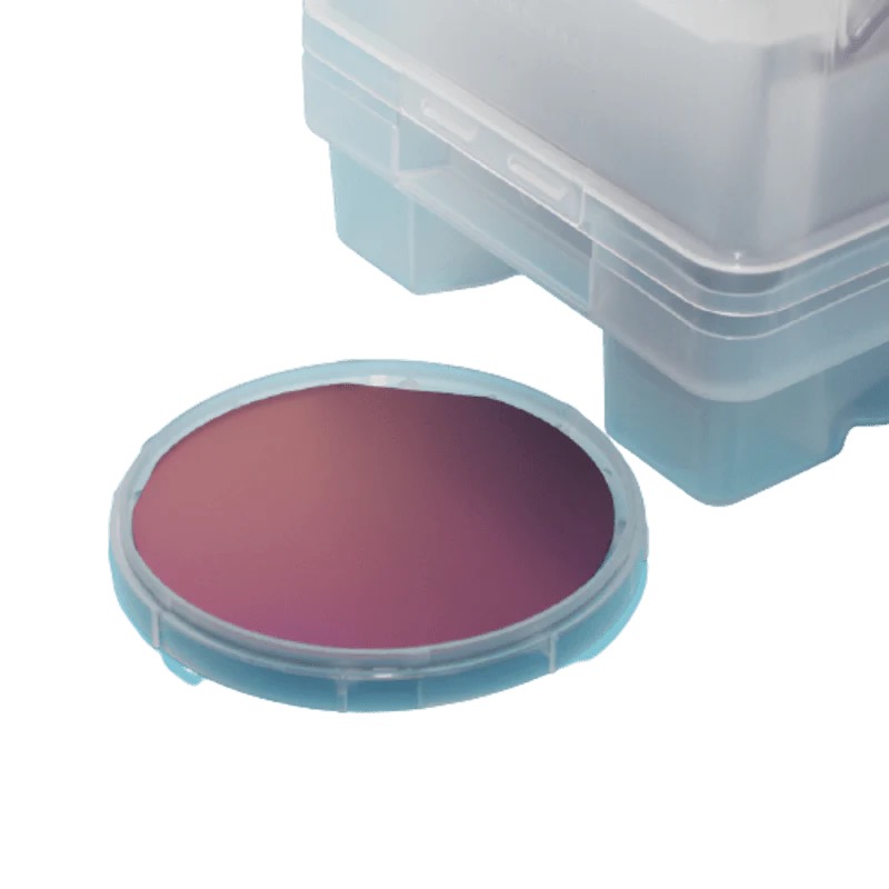
3-Inch P/N Type Silicon Wafer with Oxide Layer (1~10Ω·cm)
Optimize your semiconductor production with our 3-inch P/N Type Silicon Wafer, offering versatile resistivity (1~10Ω·cm) and a high-quality oxide layer. Designed for both P-type (boron-doped) and N-type (phosphorus/arsenic-doped) applications, this substrate ensures flexibility in fabricating diodes, transistors, and integrated circuits.
Key Features & Benefits:
Dual Conductivity Options: Choose P-type (Boron-doped) or N-type (Phosphorus-doped)substrates for tailored carrier mobility in electronic designs.
Moderate Resistivity: 1~10Ω·cm range balances conductivity and thermal stability for power devices and analog circuits.
Integrated Oxide Layer: Thermally grown SiO₂ provides insulation, surface passivation, and gate dielectric functionality.
3-Inch Standard Size: Compatible with wafer probers, lithography systems, and industrial-scale fabrication tools.
Why Choose This Wafer?
Our 3-inch P/N Type Silicon Wafer combines controlled doping precision, uniform oxide layers, and industry-standard resistivity to support diverse semiconductor workflows. Whether for prototyping or mass production, it ensures high yield and reliability in high-temperature and high-frequency environments. Trusted by engineers for advanced electronics and renewable energy solutions.