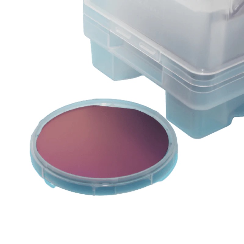
3-Inch P-Type Silicon Wafer with Oxide Layer (0.01~0.09Ω·cm)
Enhance your semiconductor manufacturing with our 3-inch P-Type Silicon Wafer, optimized for ultra-low resistivity (0.01~0.09Ω·cm) and integrated oxide layer. Designed for high-conductivity applications, this substrate ensures superior performance in power electronics, MEMS, and advanced IC production.
Key Features & Benefits:
Ultra-Low Resistivity: 0.01~0.09Ω·cm range enables efficient current flow for high-power and high-frequency devices.
P-Type Doping: Boron-doped silicon substrate for enhanced hole carrier mobility, ideal for MOSFETs, diodes, and thyristors.
Integrated Oxide Layer: Thermally grown SiO₂ layer supports insulation, passivation, and gate dielectric applications.
3-Inch Diameter: Compatible with standard semiconductor processing tools for R&D and industrial-scale production.
Why Choose This Substrate?
Our 3-inch P-Type Silicon Wafer combines precision doping, ultra-low resistivity, and a high-quality oxide layer to meet stringent industry standards. With exceptional uniformity and defect-free surfaces, it supports photolithography, etching, and thin-film deposition processes. Trusted by engineers for high-yield production and cutting-edge research in semiconductor technology.