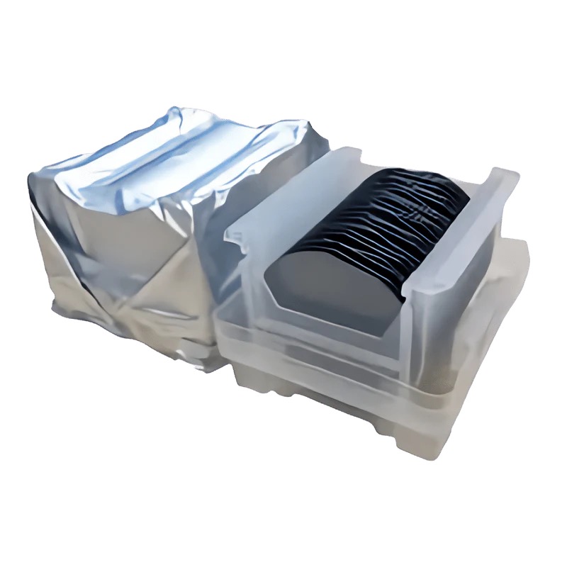
Ultra-high resistivity 4-inch FZ (100) single-sided polished silicon (R>1000Ω/10,000Ω) - the core substrate for high performance semiconductor solutions
introduction
The 4-inch floating zone (FZ) wafers are ideal for high-power, high-frequency and high-voltage semiconductor devices thanks to their **<100> crystal orientation, ultra-high resistivity (R>1000Ω·cm to 10,000Ω·cm) and single-sided polishing processes. Its unmatched purity and electrical insulation provide critical material support for RF systems, power electronics and cutting-edge research.
Core characteristic
Floating zone method (FZ) growth process:
Ultra-low impurity content: Oxygen and carbon impurities are completely removed by floating zone melting technology, and the defect density is much lower than that of CZ silicon wafers.
Perfect crystal structure: Suitable for high frequency and high voltage devices that require high material uniformity.
<100> Orientation advantage:
Uniform atomic arrangement: Support high-quality epitaxial layer growth, compatible with CMOS, MOSFET and other device processes.
Thermal stability: Withstand high temperature oxidation and annealing processes, suitable for harsh working environments.
Ultra-high resistivity (R>1000Ω·cm to 10,000Ω·cm) :
Low leakage current: Minimizes energy loss in high frequency and high voltage applications.
High breakdown voltage: High voltage power devices for electric vehicles, industrial drives and renewable energy systems.
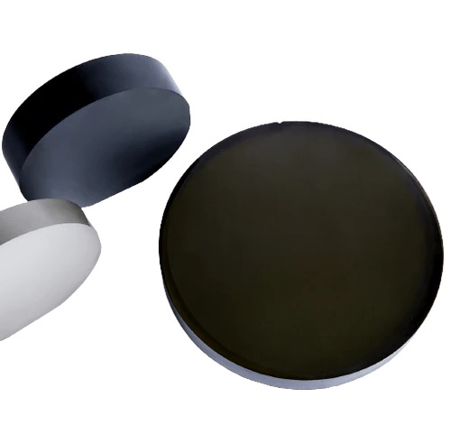
Single-side polishing process:
Mirror finish (Ra < 0.5nm) : Provides ultra-smooth surfaces for photolithography and precision device fabrication.
Back etching/grinding: Reduces costs while ensuring mechanical stability.
4 inch (100mm) diameter:
Considering cost effectiveness and equipment compatibility, it is suitable for small and medium-sized batch production and research and development.
Technological advantage
Unmatched resistivity: Meets high insulation requirements and reduces device energy consumption.
Extreme material purity: Floating zone process improves device reliability and life.
Thermal management and mechanical stability: Adaptable to high temperature processes and mechanical stress environments.
Flexible adaptation: Compatible with 4-inch production line, supporting rapid mass production and prototype development.
Technical parameter
Type: Floating Zone Method (FZ) silicon wafer
Resistivity: >1000Ω·cm to 10,000Ω·cm
Diameter: 4 inches (100mm)
Crystal direction: <100>
Thickness: 500-675µm (customizable)
Surface treatment: Single side polishing (front Ra < 0.5nm), back etching/grinding
Thickness uniformity (TTV) : <10µm
Choice reason
Industry compliance: Meets SEMI standards to ensure resistivity uniformity, flatness and surface cleanliness.
Customized services: Support resistivity range, oxide thickness and doping concentration adjustment.
Strict quality control: Defect detection and particle control ensure high yield.
Technical support: Suppliers provide process integration and optimization solutions.
Conclusion
With its <100> crystal orientation, ultra-high resistivity (R>1000Ω/10,000Ω) and single-sided polishing process, 4-inch FZ wafers are an innovative substrate for high-power, high-frequency and high-voltage semiconductor applications. Whether advancing 5G communications, new energy technologies, or exploring quantum technologies, the silicon wafer enables cutting-edge innovation with superior performance and reliability.
Take your technology projects to the next level with this ultra-high resistivity silicon wafer today!