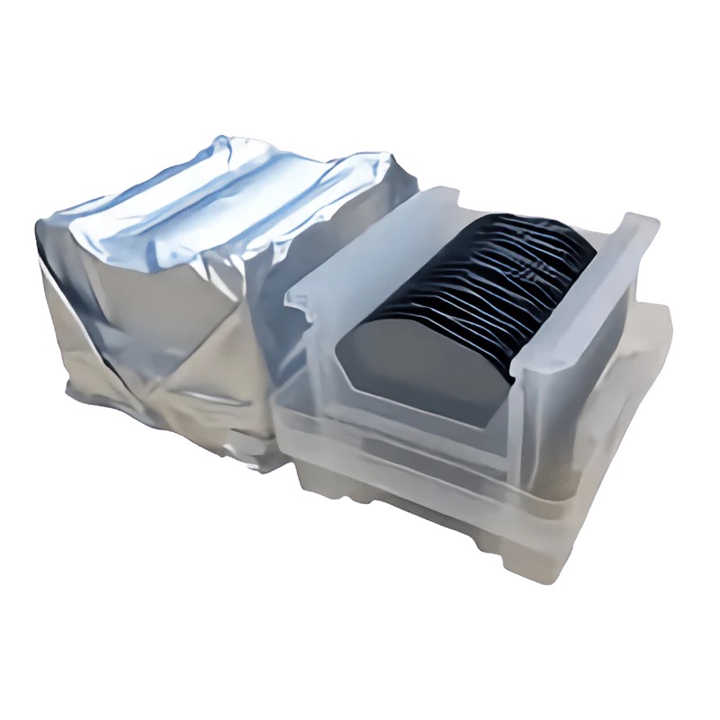
Ultra-High Resistivity 6-Inch FZ (100) Silicon Wafer with R>1000Ω/10,000Ω and Single-Side Polishing for Precision Semiconductor Solutions
Introduction
The 6-inch Float-Zone (FZ) silicon wafer with <100> crystal orientation, ultra-high resistivity (R>1000Ω·cm to 10,000Ω·cm), and single-side polishing is engineered for advanced semiconductor applications demanding extreme material purity and electrical insulation. Leveraging the superior quality of the Float-Zone process, this substrate is a cornerstone for high-frequency, high-power, and high-voltage devices. This article explores its features, applications, and competitive advantages.
Key Features
Float-Zone (FZ) Growth Method:
Ultra-High Purity: Eliminates oxygen and carbon impurities, achieving defect densities far lower than Czochralski (CZ)-grown silicon.
Exceptional Crystallinity: Ensures minimal dislocation density, critical for high-performance devices.
<100> Crystal Orientation:
Uniform Atomic Structure: Ideal for epitaxial growth, CMOS fabrication, and oxide layer integration.
Thermal and Mechanical Stability: Withstands high-temperature processing and mechanical stress in harsh environments.
Ultra-High Resistivity (R>1000Ω·cm–10,000Ω·cm):
Low Leakage Current: Minimizes energy loss in high-voltage and RF applications.
High Breakdown Voltage: Supports power devices and sensors operating under extreme electrical stress.
Single-Side Polishing:
Mirror-Polished Frontside (Ra < 0.5 nm): Ensures ultra-smooth surfaces for precision lithography and device fabrication.
Etched/Lapped Backside: Reduces costs while maintaining mechanical stability during handling and processing.
6-Inch Diameter:
Balances cost efficiency with compatibility for industrial-scale fabrication tools, supporting mid- to high-volume production.
Advantages Over Conventional Substrates
Unmatched Resistivity: Ideal for applications requiring minimal electrical conductivity and high insulation.
Material Purity: Float-Zone growth eliminates impurities, enhancing device reliability and longevity.
Thermal Resilience: Maintains structural integrity in high-temperature environments (e.g., oxidation, annealing).
Scalability: Compatible with 150mm fabrication lines for seamless integration into production workflows.
Technical Specifications
Type: Float-Zone (FZ) Silicon
Resistivity: >1000Ω·cm to 10,000Ω·cm
Diameter: 6 inches (150 mm)
Orientation: <100>
Thickness: 675–725 µm (customizable)
Surface Finish: Single-side polished (frontside), etched/lapped backside
TTV (Total Thickness Variation): < 5 µm
Why Choose This Wafer?
Industry Compliance: Meets SEMI standards for resistivity uniformity, flatness, and surface cleanliness.
Customization: Adjust resistivity ranges, oxide layers, and doping profiles for specialized needs.
Quality Assurance: Rigorous defect inspection and particle control ensure high yields in critical applications.
Technical Support: Collaborate with suppliers offering expertise in high-resistivity wafer integration.
Conclusion
The 6-inch FZ silicon wafer with <100> orientation, ultra-high resistivity (R>1000Ω/10,000Ω), and single-side polishing is a game-changer for high-power, high-frequency, and high-voltage semiconductor applications. Its unparalleled purity, electrical insulation, and thermal stability make it indispensable for RF systems, power electronics, radiation detection, and cutting-edge research. Whether scaling prototypes or optimizing industrial production, this wafer delivers the precision, reliability, and performance needed to push technological boundaries.
Elevate your semiconductor innovations with this ultra-high-resistivity, industry-leading substrate today!