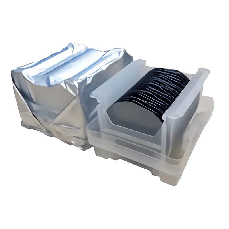
Premium 4-Inch FZ N-Type Silicon Wafer (111 Orientation) 50~70Ω·cm with Single-Side Polishing for High-Performance Semiconductor Devices
Introduction
The 4-inch Float-Zone (FZ) N-type silicon wafer with <111> crystal orientation, 50–70Ω·cm resistivity, and single-side polishing is engineered for high-performance semiconductor applications requiring ultra-low defect density and exceptional electrical properties. Leveraging the superior purity of the Float-Zone method, this substrate is ideal for RF components, power devices, and precision sensors. This article explores its features, applications, and advantages in advanced electronics.
Key Features
Float-Zone (FZ) Growth Method:
Ultra-High Purity: Removes impurities and oxygen content, achieving defect densities far lower than Czochralski (CZ)-grown silicon.
Exceptional Crystallinity: Ideal for high-frequency and high-power devices where material quality directly impacts performance.
<111> Crystal Orientation:
Anisotropic Etching Compatibility: Enables precise 3D microstructures for MEMS, sensors, and specialized optoelectronic devices.
High Atomic Density: Enhances mechanical stability and thermal resistance in demanding environments.
Resistivity (50–70Ω·cm):
Optimized for applications requiring moderate conductivity, balancing electron mobility and leakage current control.
Single-Side Polishing:
Mirror-Polished Frontside (Ra < 0.5 nm): Ensures ultra-smooth surfaces for high-precision lithography and device fabrication.
Etched/Lapped Backside: Reduces costs while maintaining mechanical stability during processing.
4-Inch Diameter:
Cost-effective for prototyping and small-to-medium volume production, compatible with 100mm fabrication tools.
Advantages Over CZ-Grown Wafers
Lower Defect Density: Minimizes leakage currents and enhances device reliability.
Higher Thermal Conductivity: Improves heat dissipation in high-power applications.
Anisotropic Etching Precision: Achieves superior geometric control for MEMS and sensors.
Cost Efficiency: Single-side polishing balances performance and affordability.
Technical Specifications
Type: N-type (Phosphorus/Arsenic-doped)
Growth Method: Float-Zone (FZ)
Resistivity: 50–70 Ω·cm
Diameter: 4 inches (100 mm)
Orientation: <111>
Thickness: 500–675 µm (standard)
Surface Finish: Single-side polished (frontside), etched/lapped backside
TTV (Total Thickness Variation): < 10 µm
Why Choose This Wafer?
Industry Compliance: Meets SEMI standards for resistivity uniformity, flatness, and surface cleanliness.
Customization: Adjust resistivity, doping profiles, and oxide layers for specialized needs.
Quality Assurance: Rigorous defect inspection ensures high yields in critical applications.
Technical Support: Partner with suppliers offering expertise in FZ wafer processing and integration.
Conclusion
The 4-inch FZ N-type silicon wafer with <111> orientation, 50–70Ω·cm resistivity, and single-side polishing is a cornerstone of advanced semiconductor manufacturing. Its unparalleled purity, precise crystal structure, and surface quality make it indispensable for RF, power electronics, MEMS, and optoelectronic applications. Whether for prototyping or scaling production, this wafer delivers the performance, reliability, and versatility needed to drive next-generation innovations.
Elevate your semiconductor projects with this ultra-pure, high-performance substrate today!