High-Performance 4-Inch N-Type Silicon Wafer (111 Orientation) with Single/Double-Side Polishing for Advanced Semiconductor Applications
Introduction
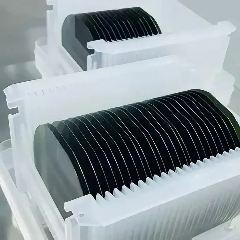
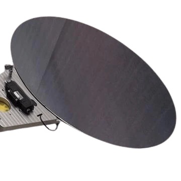
The 4-inch N-type silicon wafer with <111> crystal orientation and single/double-side polishing is a specialized substrate engineered for precision semiconductor applications. Combining superior electrical properties, atomic alignment, and surface quality, this wafer is pivotal for industries such as microelectromechanical systems (MEMS), power electronics, and optoelectronics. This article explores its features, applications, and competitive advantages.
Key Features
<111> Crystal Orientation:
High Atomic Density and Anisotropic Etching: The <111> orientation enables precise geometric control in wet chemical etching, making it ideal for MEMS devices, sensors, and 3D microstructures.
Compatibility with Epitaxial Growth: Supports high-quality epitaxial layers for advanced compound semiconductor devices (e.g., GaN-on-Si).
Single/Double-Side Polishing Options:
Single-Side Polishing: Frontside mirror finish (Ra < 0.5 nm) ensures ultra-smooth device fabrication; backside etched or lapped for cost efficiency.
Double-Side Polishing: Both sides polished (Ra < 0.3 nm) for bidirectional precision in photonics, advanced sensors, and optical components.
N-Type Doping (Phosphorus/Arsenic):
High electron mobility and low resistivity (0.001–0.02 ohm-cm) for high-speed transistors, RF components, and power devices.
High Purity and Low Defect Density:
Produced via Czochralski (CZ) or Float-Zone (FZ) methods, ensuring minimal impurities and crystal defects for reliable performance.
4-Inch Diameter:
Cost-effective for prototyping and small-to-medium volume production while remaining compatible with 100mm fabrication tools.
Advantages Over Competing Substrates
Anisotropic Etching Precision: Achieve complex geometries in MEMS and sensors with <111> orientation.
Polishing Flexibility: Choose cost-efficient single-side polishing or high-precision double-side polishing.
Thermal Stability: Withstands high-temperature processes like oxidation, diffusion, and annealing.
Scalability: Compatible with 100mm production lines for seamless integration into existing workflows.
Technical Specifications
Type: N-type (Phosphorus/Arsenic-doped)
Resistivity Range: 0.001–0.02 ohm-cm (customizable)
Diameter: 4 inches (100 mm)
Orientation: <111>
Thickness: 500–675 µm (standard)
Surface Finish: Single/double-side polished (Ra < 0.5 nm / < 0.3 nm)
TTV (Total Thickness Variation): < 10 µm
Why Choose This Wafer?
Industry Compliance: Meets SEMI standards for flatness, resistivity uniformity, and surface cleanliness.
Customization: Adjust doping levels, oxide layers, and thickness for niche applications.
Quality Assurance: Rigorous defect inspection ensures high yields in demanding fabrication processes.
Technical Support: Collaborate with suppliers for doping optimization and surface engineering guidance.
Conclusion
The 4-inch N-type silicon wafer with <111> crystal orientation and single/double-side polishing is a critical enabler of cutting-edge semiconductor innovation. Its unique atomic structure, exceptional surface quality, and electrical performance make it indispensable for MEMS, power electronics, optoelectronics, and RF applications. Whether scaling prototypes or optimizing high-volume production, this wafer delivers the precision, reliability, and versatility needed to drive technological advancements.
Enhance your semiconductor projects with this high-performance, customizable substrate today!