Versatile 4-Inch P-Type Silicon Wafer (100 Orientation) with Single/Double-Side Polishing for Precision Semiconductor Solutions
Introduction
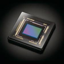
The 4-inch P-type silicon wafer with <100> crystal orientation and single/double-side polishing is a foundational substrate for diverse semiconductor applications. Combining exceptional electrical performance, surface quality, and flexibility, this wafer meets the demands of industries ranging from microelectronics to renewable energy. This article explores its features, applications, and advantages in modern technology.
Key Features
<100> Crystal Orientation:
A standard orientation for semiconductor devices, offering uniform atomic structure for epitaxial growth, oxide layer formation, and compatibility with CMOS, MOSFETs, and MEMS fabrication.
Single/Double-Side Polishing Options:
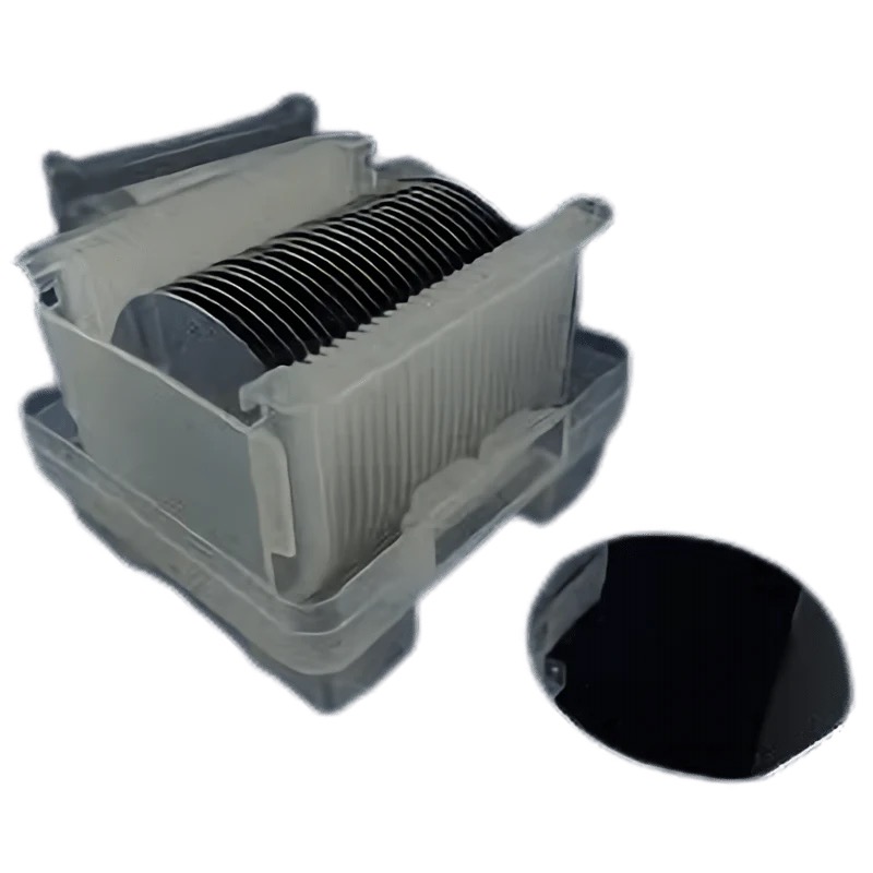
Single-Side Polishing: Frontside mirror-polished (Ra < 0.5 nm) for smooth device fabrication; backside etched or lapped for cost efficiency.
Double-Side Polishing: Ultra-smooth surfaces on both sides (Ra < 0.3 nm) for applications requiring bidirectional precision, such as photonics or advanced sensors.
P-Type Doping (Boron):
Adjustable resistivity (1–100 ohm-cm) ensures precise hole conduction for analog circuits, power devices, and photovoltaic cells.
High Purity and Low Defect Density:
Manufactured via Czochralski (CZ) or Float-Zone (FZ) methods, ensuring minimal impurities and crystal defects for reliable performance.
4-Inch Diameter:
Cost-effective for prototyping and small-to-medium volume production while remaining compatible with 100mm fabrication tools.
Advantages Over Competing Substrates
Polishing Flexibility: Choose single-side for cost efficiency or double-side for bidirectional precision.
Thermal and Chemical Stability: Withstands high-temperature processes (e.g., oxidation, diffusion) and harsh chemical environments.
Customization: Adjust resistivity, oxide layers, and thickness (e.g., 500–1000 µm) for niche applications.
Scalability: Compatible with 100mm production lines for seamless integration into existing workflows.
Technical Specifications
Type: P-type (Boron-doped)
Resistivity Range: 1–100 ohm-cm (customizable)
Diameter: 4 inches (100 mm)
Orientation: <100>
Thickness: 500–1000 µm (standard)
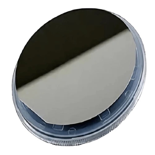
Surface Finish: Single/double-side polished (Ra < 0.5 nm / < 0.3 nm)
TTV (Total Thickness Variation): < 10 µm
Why Choose This Wafer?
Industry Compliance: Meets SEMI standards for flatness, resistivity uniformity, and surface cleanliness.
Cost Efficiency: Single-side polishing reduces costs; double-side polishing enhances performance for high-end applications.
Quality Assurance: Rigorous defect inspection ensures high yields in demanding fabrication processes.
Technical Support: Partner with suppliers offering doping optimization and surface engineering guidance.
Conclusion
The 4-inch P-type silicon wafer with <100> crystal orientation and single/double-side polishing is a cornerstone of semiconductor innovation. Its adaptability, superior surface quality, and electrical performance make it indispensable for MEMS, power electronics, optoelectronics, and research. Whether optimizing prototypes or scaling production, this wafer delivers the precision, reliability, and versatility needed to drive technological advancements.
Upgrade your semiconductor projects with this high-performance, customizable substrate today!