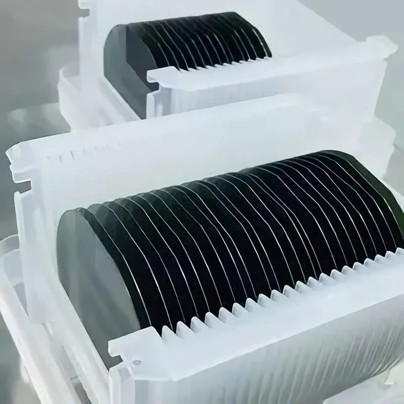
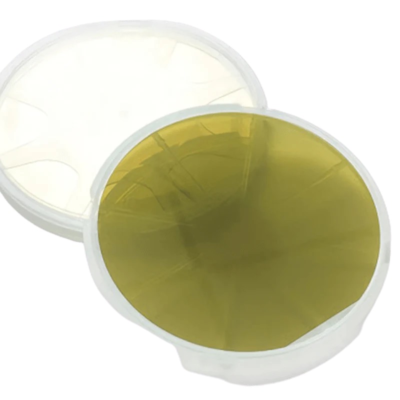
Silicon wafer 6inch N Type(100/111) Single Side Polished Semiconductor Substrate
Introduction
The 6-inch N-type silicon wafer with <100> or <111> crystal orientation and single-side polishingis a cornerstone of modern semiconductor manufacturing. Designed for high-performance electronic and optoelectronic applications, this substrate combines exceptional crystallinity, surface quality, and electrical properties. This article examines its features, applications, and advantages in cutting-edge technology.
Key Features of the 6-Inch N-Type Silicon Wafer
Crystal Orientation Options (<100> and <111>):
<100> Orientation: Preferred for MOSFETs, CMOS sensors, and epitaxial growth due to its uniform surface structure and compatibility with oxide layers.
<111> Orientation: Ideal for specialized MEMS devices, bipolar transistors, and certain optoelectronic applications requiring higher atomic density.
Single-Side Polishing:
One side is mirror-polished (Ra < 0.5 nm) for ultra-smooth device fabrication, while the backside remains unpolished for cost efficiency or mechanical handling.
N-Type Doping (Phosphorus/Arsenic):
Offers high electron mobility and low resistivity (adjustable doping levels) for high-speed transistors, power devices, and RF components.
High Purity and Low Defect Density:
Produced via Czochralski (CZ) or Float-Zone (FZ) methods, ensuring minimal dislocations and impurities for reliable device performance.
6-Inch Diameter:
Balances cost-effectiveness and compatibility with industrial fabrication tools, enabling scalable production for mid- to high-volume applications.
Advantages Over Competing Substrates
Orientation Flexibility: Choose <100> for standard ICs or <111> for MEMS/optoelectronics.
Cost-Effective Polishing: Single-side polishing reduces production costs without compromising surface quality.
Thermal and Mechanical Stability: High-purity silicon ensures durability in high-temperature processes.
Scalability: Compatible with 150mm fabrication lines for seamless integration into existing workflows.
Technical Specifications
Type: N-type (Phosphorus/Arsenic-doped)
Resistivity: Customizable (e.g., 0.001–0.02 ohm-cm)
Diameter: 6 inches (150 mm)
Orientation: <100> or <111>
Thickness: 525–675 µm (standard)
Surface Finish: Single-side polished (frontside), etched or lapped backside
TTV (Total Thickness Variation): < 5 µm
Why Choose This Wafer?
Industry Compliance: Meets SEMI standards for flatness, resistivity uniformity, and particle control.
Customization: Adjust doping levels, orientation, and thickness for niche applications.
Quality Assurance: Rigorous inspection for defects, ensuring high yield in device fabrication.
Conclusion
The 6-inch N-type silicon wafer with <100>/<111> orientation and single-side polishing is a versatile, high-performance substrate for next-generation semiconductor devices. Its tailored crystal structure, superior surface quality, and compatibility with industrial processes make it indispensable for power electronics, MEMS, RF systems, and beyond. Whether for prototyping or mass production, this wafer delivers the precision and reliability needed to drive innovation.
Enhance your semiconductor projects with this industry-leading silicon substrate today!