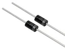
High-Performance 4-Inch P-Type Silicon Wafer (111 Orientation) with Single-Side Polishing for Precision Semiconductor Applications
Introduction
The 4-inch P-type silicon wafer with <111> crystal orientation and single-side polishing is a specialized substrate designed for applications demanding precise atomic alignment and exceptional surface quality. Combining robust electrical properties with mechanical stability, this wafer is a cornerstone for advanced semiconductor devices in industries ranging from microelectronics to renewable energy. This article delves into its features, applications, and competitive advantages.
Key Features of the 4-Inch P-Type (111) Silicon Wafer
<111> Crystal Orientation:
Known for its high atomic density and anisotropic etching properties, the <111> orientation is ideal for MEMS devices, bipolar transistors, and optoelectronic components requiring precise geometric control.
Provides excellent compatibility with wet chemical etching and epitaxial growth processes.
Single-Side Polishing:
Frontside Polishing: Mirror-smooth surface (Ra < 0.5 nm) ensures minimal scattering and defects for high-precision device fabrication.
Backside Etching/Lapping: Enhances mechanical stability during handling and reduces production costs.
P-Type Doping (Boron):
Achieves controlled hole conduction with adjustable resistivity (e.g., 1–50 ohm-cm), tailored for analog circuits, power devices, and photovoltaics.
High Purity and Low Defect Density:
Produced via the Czochralski (CZ) method, ensuring uniform crystal structure and minimal impurities for reliable device performance.
4-Inch Diameter:
Cost-effective format compatible with legacy and specialized fabrication tools, ideal for prototyping and small-to-medium volume production.
Advantages Over Conventional Substrates
Anisotropic Etching Compatibility: Enables precise geometric patterning for MEMS and sensors.
Thermal Stability: Withstands high-temperature processes like oxidation and diffusion.
Cost Efficiency: Single-side polishing reduces manufacturing costs without compromising device-side quality.
Mechanical Durability: Thicker substrates (e.g., 525–675 µm) resist warping in harsh environments.
Technical Specifications
Type: P-type (Boron-doped)
Resistivity Range: 1–50 ohm-cm (customizable)
Diameter: 4 inches (100 mm)
Orientation: <111>
Thickness: 525–675 µm (standard)
Surface Finish: Single-side polished (front), etched/lapped backside
TTV (Total Thickness Variation): < 10 µm
Why Choose This Wafer?
Industry Compliance: Meets SEMI standards for thickness uniformity (±2.5%), flatness, and surface cleanliness.
Customization: Adjust resistivity, oxide layers, and thickness for niche applications.
Quality Assurance: Rigorous defect inspection ensures high yields in demanding fabrication processes.
Conclusion
The 4-inch P-type silicon wafer with <111> crystal orientation and single-side polishing is a critical enabler of precision semiconductor innovation. Its unique atomic structure, coupled with superior electrical and mechanical properties, makes it indispensable for MEMS, power electronics, optoelectronics, and cutting-edge research. Whether scaling prototypes or optimizing specialized devices, this wafer delivers the performance, reliability, and cost efficiency needed to push technological boundaries.
Upgrade your semiconductor projects with this high-performance <111> silicon substrate today!