4-Inch P-Type Silicon Wafer (100 Orientation) with 1-10Ω Resistivity and Custom Thickness (1000µm/3000µm/5000µm) for Robust Semiconductor Applications
Introduction
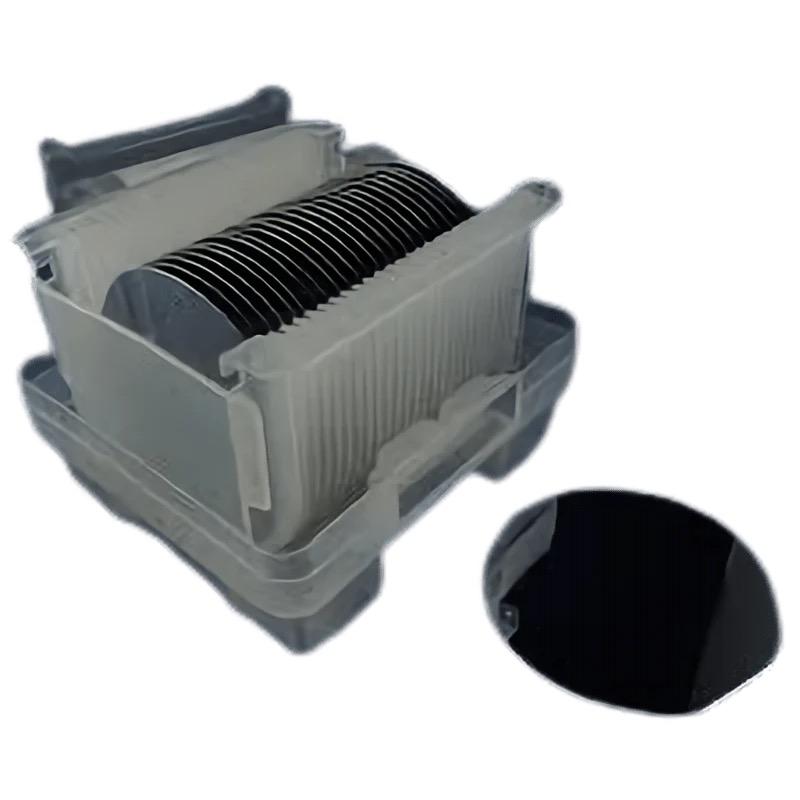
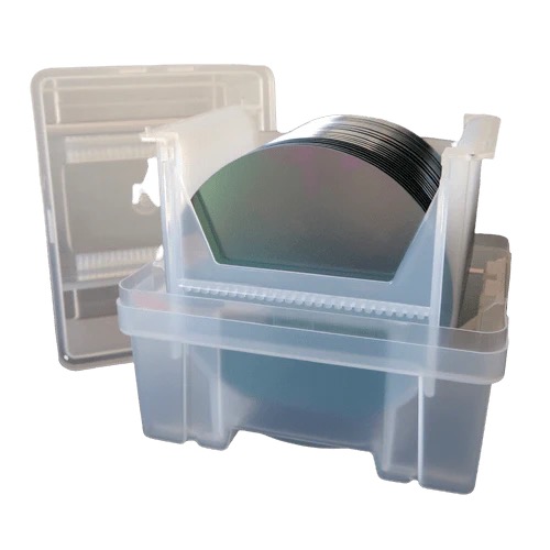
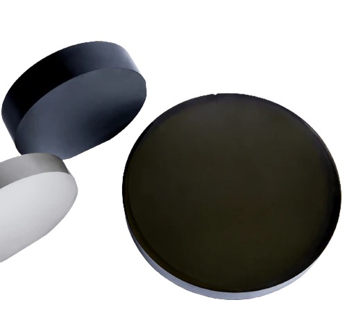
The 4-inch P-type silicon wafer with <100> crystal orientation, 1-10Ω·cm resistivity, and custom thickness options (1000µm/3000µm/5000µm) is engineered to meet the demands of specialized semiconductor and microelectronics applications. Featuring single-side polishing and robust mechanical stability, this substrate is ideal for industries requiring precise electrical performance and durability. This article explores its features, applications, and advantages.
Key Features
<100> Crystal Orientation:
A standard orientation for semiconductor devices, offering uniform atomic structure for epitaxial growth, oxide layer formation, and compatibility with CMOS and MEMS fabrication processes.
Adjustable Resistivity (1-10Ω·cm):
Boron-doped P-type silicon provides precise hole conduction, tailored for applications requiring moderate to high resistivity, such as sensors and analog circuits.
Custom Thickness Options:
1000µm (1mm): Standard thickness for general-purpose ICs and optoelectronics.
3000µm (3mm): Enhanced mechanical strength for high-power devices or harsh environments.
5000µm (5mm): Ultra-thick for specialized MEMS, sensors, or substrates requiring minimal warping.
Single-Side Polishing:
Mirror-polished front surface (Ra < 0.5 nm) ensures smooth device fabrication, while the unpolished backside aids mechanical handling or cost efficiency.
High Purity & Durability:
Manufactured via Czochralski (CZ) method, ensuring low defect density and thermal stability for high-temperature processing.
Advantages Over Conventional Substrates
Thickness Versatility: Choose 1000µm, 3000µm, or 5000µm to balance mechanical strength and process compatibility.
Cost Efficiency: Single-side polishing reduces production costs without compromising device-side quality.
Thermal Resilience: Withstands oxidation, diffusion, and annealing processes.
Scalability: Compatible with 100mm fabrication tools for prototyping and mid-volume production.
Technical Specifications
Type: P-type (Boron-doped)
Resistivity: 1–10 ohm-cm (customizable)
Diameter: 4 inches (100 mm)
Thickness: 1000µm / 3000µm / 5000µm
Orientation: <100>
Surface Finish: Single-side polished (front), etched/lapped backside
TTV (Total Thickness Variation): < 10µm
Why Choose This Wafer?
Industry Compliance: Meets SEMI standards for resistivity uniformity, flatness, and surface cleanliness.
Tailored Solutions: Customize resistivity, thickness, and doping profiles for niche applications.
Quality Assurance: Rigorous defect inspection ensures high yield in demanding environments.
Conclusion
The 4-inch P-type silicon wafer with <100> orientation, 1-10Ω·cm resistivity, and 1000µm/3000µm/5000µm thickness options is a versatile and reliable substrate for advanced semiconductor applications. Its adaptability to diverse thickness requirements, coupled with excellent electrical and mechanical properties, makes it indispensable for MEMS, power devices, sensors, and R&D. Whether prototyping or scaling production, this wafer delivers the precision and durability needed for next-generation technologies.
Enhance your semiconductor projects with this customizable, high-performance substrate today!