Premium 6-Inch P-Type Silicon Wafer (100/111 Orientation) with Single-Side Polishing for High-Performance Semiconductor Devices
Introduction
The 6-inch P-type silicon wafer with <100> or <111> crystal orientation and single-side polishingis a critical substrate for advanced semiconductor applications. Engineered to deliver exceptional electrical performance and surface quality, this wafer is tailored for industries ranging from consumer electronics to renewable energy. This article explores its features, applications, and competitive advantages.
Key Features of the 6-Inch P-Type Silicon Wafer
Crystal Orientation Flexibility (<100> and <111>):
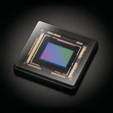
<100> Orientation: Widely used in CMOS sensors, MOSFETs, and integrated circuits (ICs) due to its uniform surface structure and compatibility with oxide layers.
<111> Orientation: Preferred for MEMS devices, bipolar transistors, and certain optoelectronic applications requiring higher atomic density and anisotropic etching properties.
Single-Side Polishing:
The front side is mirror-polished (surface roughness Ra < 0.5 nm) to ensure ultra-smooth device fabrication, while the backside remains unpolished for cost efficiency or mechanical stability during processing.
P-Type Doping (Boron):
Achieves precise hole conduction with adjustable resistivity (e.g., 1–50 ohm-cm), making it ideal for analog circuits, power devices, and photovoltaics.
High Purity and Low Defect Density:
Manufactured via Czochralski (CZ) or Float-Zone (FZ) methods, ensuring minimal impurities and crystal defects for reliable device performance.
6-Inch Diameter Compatibility:
Balances cost-efficiency with compatibility for industrial fabrication equipment, supporting scalable production for mid- to high-volume applications.
Advantages Over Competing Substrates
Dual-Orientation Versatility: Optimize performance for specific applications by selecting <100> or <111> crystal planes.
Cost-Effective Surface Finish: Single-side polishing reduces manufacturing costs without compromising device-side quality.
Thermal and Chemical Stability: Withstands high-temperature processes and harsh chemical environments.
Scalability: Compatible with 150mm production lines, facilitating seamless integration into existing workflows.
Technical Specifications
Type: P-type (Boron-doped)
Resistivity Range: 1–50 ohm-cm (customizable)
Diameter: 6 inches (150 mm)
Orientation: <100> or <111>
Thickness: 525–675 µm (standard)
Surface Finish: Single-side polished (frontside), etched or lapped backside
TTV (Total Thickness Variation): < 5 µm
Why Choose This Wafer?
Industry Compliance: Meets SEMI standards for thickness uniformity (±2.5%), flatness, and surface cleanliness.
Customization Options: Tailor resistivity, orientation, and oxide layer thickness to meet specific project requirements.
Quality Assurance: Rigorous defect inspection and particle control ensure high yields in device fabrication.
Conclusion
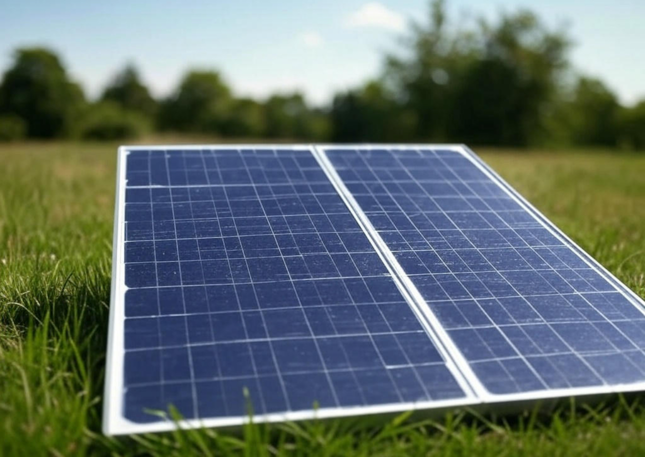
The 6-inch P-type silicon wafer with <100>/<111> crystal orientation and single-side polishing is a cornerstone of modern semiconductor innovation. Its adaptability, superior electrical properties, and compatibility with industrial processes make it indispensable for applications in electronics, MEMS, solar energy, and beyond. Whether for prototyping or mass production, this wafer delivers the precision, reliability, and cost efficiency needed to drive technological advancements.
Elevate your semiconductor projects with this high-performance P-type silicon substrate today!