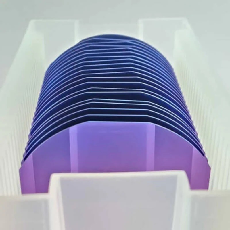
Versatile 4-Inch P/N-Type Silicon Wafers with Ultra-Low Resistivity (0.001–0.005Ω) and Oxide Layer for Precision Semiconductor Solutions
Introduction
In the semiconductor industry, the choice of substrate material directly impacts device efficiency and functionality. The 4-inch P/N-type silicon wafer with ultra-low resistivity (0.001–0.005Ω) and a tailored oxide layer offers unmatched versatility for cutting-edge applications. This article delves into its design, applications, and why it’s a preferred choice for engineers and manufacturers.
Key Features of the 4-Inch P/N-Type Silicon Wafer
Ultra-Low Resistivity Range (0.001–0.005Ω):
P-Type (Boron-Doped): Ideal for applications requiring hole conduction, such as CMOS sensors and analog circuits.
N-Type (Phosphorus/Arsenic-Doped): Optimized for electron mobility, perfect for high-speed transistors and power devices.
Broad resistivity range accommodates diverse voltage and current requirements.
Precision Oxide Layer (SiO₂):
Enhances insulation, surface passivation, and chemical stability.
Oxide thickness customizable from 50 nm to 1,000 nm for gate dielectrics, masking, or protective coatings.
High Purity and Crystal Quality:
Produced via Czochralski (CZ) or Float-Zone (FZ) methods, ensuring minimal defects and exceptional uniformity.
Polished surfaces (single/double-side) reduce scattering losses in optoelectronic devices.
4-Inch Diameter Compatibility:
Balances cost-effectiveness with compatibility for legacy and specialized fabrication tools.
Advantages Over Conventional Substrates
Dual-Type Flexibility: Choose P-type for CMOS/analog or N-type for high-frequency/power applications.
Thermal and Electrical Stability: Oxide layer improves heat dissipation and reduces surface recombination.
Customizable Doping Profiles: Tailor resistivity and oxide thickness to meet specific design needs.
Scalability: Suitable for prototyping, pilot runs, and large-scale production.
Technical Specifications
Type: P-type (Boron-doped) / N-type (Phosphorus/Arsenic-doped)
Resistivity: 0.001–0.005 ohm-cm (adjustable)
Diameter: 4 inches (100 mm)
Orientation: <100> or <111>
Oxide Thickness: 50–1,000 nm (customizable)
Surface Finish: Single/double-side polished
Why Choose This Wafer?
Industry Compliance: Meets SEMI standards for thickness tolerance (±2.5%) and surface roughness (<1 nm).
Reliability: Rigorous defect inspection ensures consistent performance in harsh environments.
Technical Support: Collaborate with suppliers offering doping optimization and oxide layer engineering.
Conclusion
The 4-inch P/N-type silicon wafer with ultra-low resistivity (0.001–0.005Ω) and precision oxide layer is a cornerstone of modern semiconductor innovation. Its dual-type versatility, coupled with tailored electrical and thermal properties, makes it indispensable for power electronics, MEMS, optoelectronics, and beyond. Whether for R&D or mass production, this substrate delivers the precision, efficiency, and scalability required to drive next-generation technologies.
Upgrade your semiconductor solutions with this high-performance wafer today!