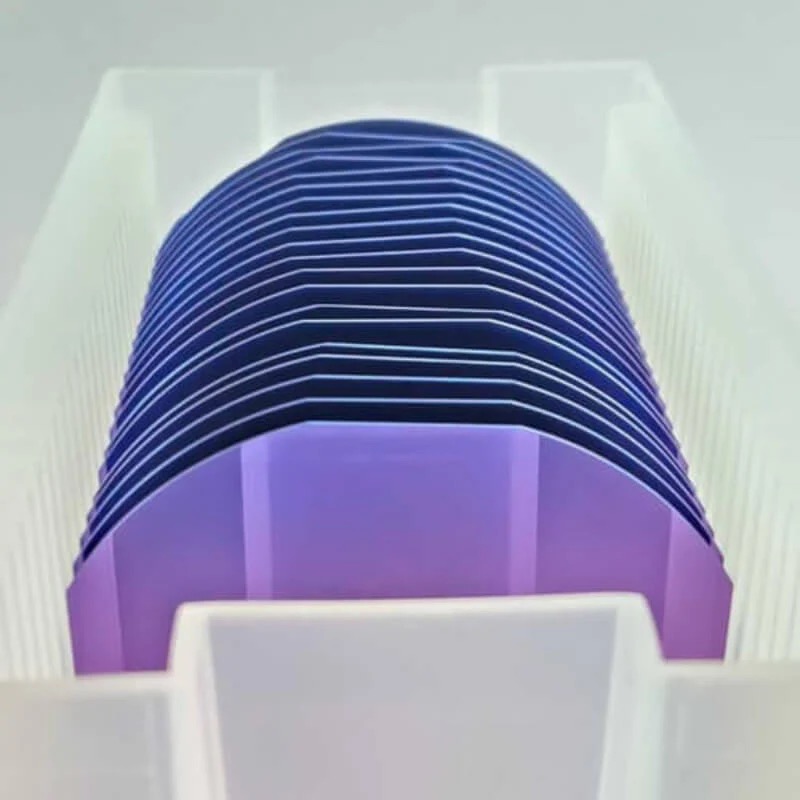
High-Performance 4-Inch N-Type Silicon Wafer with Ultra-Low Resistance (0.002–0.004Ω) and Oxide Layer for Advanced Semiconductor Applications
Introduction
In the rapidly evolving semiconductor industry, the demand for high-performance substrates continues to grow. The 4-inch N-type silicon wafer with ultra-low resistivity (0.002–0.004Ω) and a precision-engineered oxide layer stands out as a critical component for advanced electronic and optoelectronic applications. This article explores its unique properties, applications, and advantages in modern technology.
Key Features of the 4-Inch N-Type Silicon Wafer
Ultra-Low Resistivity (0.002–0.004Ω):
Achieved through heavy doping with elements like phosphorus or arsenic, this wafer ensures minimal electrical resistance, making it ideal for high-current applications such as power devices and high-frequency circuits.
Precision Oxide Layer:
A uniform silicon dioxide (SiO₂) layer provides excellent insulation, surface passivation, and protection against contamination. The oxide thickness can be customized for specific uses, including gate dielectrics or masking layers.
High Purity and Crystallinity:
Manufactured using Czochralski (CZ) or Float-Zone (FZ) methods, the wafer guarantees exceptional crystal structure integrity, reducing defects and enhancing device performance.
4-Inch Diameter Compatibility:
Compatible with legacy and specialized fabrication equipment, this wafer bridges cost efficiency and industrial scalability.
Advantages Over Competing Substrates
Enhanced Conductivity: Ultra-low resistivity minimizes energy loss in high-power applications.
Thermal Stability: The oxide layer improves heat dissipation and device longevity.
Customizability: Tailored doping profiles and oxide thicknesses meet diverse industrial needs.
Technical Specifications
Type: N-type (Phosphorus/Arsenic-doped)
Resistivity: 0.002–0.004 ohm-cm
Diameter: 4 inches (100mm)
Orientation: <100> or <111>
Oxide Thickness: 50–1000 nm (customizable)
Surface Finish: Single-side or double-side polished
Why Choose This Wafer?
Strict Quality Control: Meets SEMI and industry standards for thickness uniformity and surface roughness.
Scalable Production: Suitable for R&D prototyping and mass production.
Technical Support: Partner with suppliers offering application-specific guidance.
Conclusion
The 4-inch N-type silicon wafer with 0.002–0.004Ω resistivity and oxide layer is a cornerstone of modern semiconductor innovation. Its blend of ultra-low resistance, thermal resilience, and process adaptability makes it indispensable for next-gen electronics. Whether for power systems, MEMS, or optoelectronics, this substrate delivers unparalleled performance and reliability.
Optimize your semiconductor projects today with this cutting-edge silicon wafer!