Ultra-Low Resistivity 4-Inch N-Type Silicon Wafers (0.01–0.02Ω·cm) with Oxide Layer: Powering High-Performance Semiconductor Devices
Introduction
In the realm of high-power and high-frequency semiconductor applications, material performance is non-negotiable. 4-inch N-type silicon wafers with ultra-low resistivity (0.01–0.02Ω·cm) and integrated oxide layers are engineered to meet these demands. This article delves into their specifications, manufacturing innovations, and transformative roles in cutting-edge technologies.
1. Product Overview
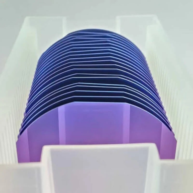
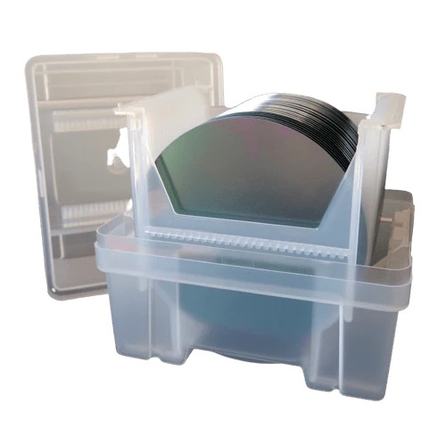
4-inch N-type silicon wafers are fabricated using high-purity monocrystalline silicon, doped with phosphorus (P) or arsenic (As) to achieve ultra-low resistivity (0.01–0.02Ω·cm). These wafers feature a thermally grown oxide layer (SiO₂) (100–500nm), providing critical insulation and surface passivation for high-voltage and high-frequency operations.
2. Key Specifications
Resistivity: 0.01–0.02Ω·cm (±3% uniformity) for minimal conduction losses.
Diameter/Thickness: 4-inch (100mm), 525±25µm.
Crystal Orientation: <100> or <111> with defect density <300 EPI.
Oxide Layer: 100–500nm SiO₂ via dry/wet oxidation, breakdown voltage >15 MV/cm.
Surface Finish: Double-side polished (Ra <0.3nm) for epitaxial growth compatibility.
3. Core Advantages
Ultra-Low Resistivity: Enables high current density and reduced heat generation in power devices.
Superior Oxide Quality: Enhances dielectric strength and device longevity.
High Thermal Conductivity: Efficient heat dissipation for high-power applications.
Strict Quality Compliance: Meets SEMI/ASTM standards, verified via Hall effect measurements and C-V profiling.
4. Manufacturing Excellence
Czochralski (CZ) Growth: Produces dislocation-free silicon crystals for ultra-low resistivity.
Precision Doping: Ion implantation ensures controlled carrier concentration (1e19–1e20 atoms/cm³).
Thermal Oxidation: Dry O₂ oxidation for dense SiO₂ layers; wet oxidation for faster growth.
Metrology: Four-point probe (resistivity), spectroscopic ellipsometry (oxide thickness), and X-ray topography (crystallinity).
5. Market Trends & Innovations
The surge in electric vehicles, 5G infrastructure, and renewable energy systems is driving demand for ultra-low resistivity silicon wafers. These wafers bridge the gap between traditional silicon and wide-bandgap materials (e.g., GaN, SiC), offering a cost-effective solution for hybrid power modules. Innovations like patterned oxide layers and backside metallization further enhance their versatility.
Conclusion
4-inch N-type silicon wafers with 0.01–0.02Ω·cm resistivity and oxide layers are pivotal in advancing high-efficiency semiconductor technologies. Their unmatched electrical performance and reliability make them indispensable for next-generation power electronics, RF systems, and automotive innovations.