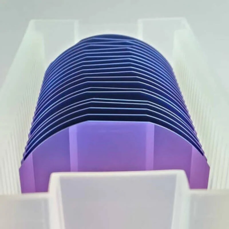
4-Inch P/N-Type Silicon Wafers (1–10Ω·cm) with Oxide Layer: Key Specifications and Applications in Advanced Semiconductor Devices
Introduction
Silicon wafers are foundational to modern electronics. This article explores 4-inch P/N-type silicon wafers with 1–10Ω·cm resistivity and integrated oxide layers, highlighting their technical specifications, manufacturing processes, and diverse industrial applications.
1. Product Overview
Conductivity Types: Available in P-type (Boron-doped) and N-type (Phosphorus/Arsenic-doped) variants for tailored electrical properties.
Resistivity Range: Optimized 1–10Ω·cm for low-power loss and high-speed performance in devices.
Oxide Layer: Thermally grown SiO₂ (100–1000nm thickness) for insulation, surface passivation, and compatibility with photolithography.
2. Key Specifications
Diameter: 4-inch (100mm) with thickness 525±25µm.
Orientation: <100> or <111> crystal orientation, defect density <500/cm².
Surface Finish: Double-side polished (Ra <0.5nm) or single-side oxidized.
Resistivity Uniformity: ±5% across the wafer.
Oxide Quality: Breakdown voltage >10MV/cm, low interface trap density.
3. Technical Advantages
Precision Doping: Ion implantation or diffusion ensures controlled carrier concentration.
Thermal Oxide Stability: Enhances dielectric strength and reduces leakage currents.
Cost-Efficiency: Ideal for R&D and mid-scale production of analog/digital ICs.
Versatility: Compatible with CMOS, BiCMOS, and MEMS fabrication processes.
4. Manufacturing Insights
Oxidation Process: Dry/wet thermal oxidation for tailored SiO₂ thickness and density.
Quality Assurance: ASTM/SEMI-compliant testing via four-point probe (resistivity), ellipsometry (oxide thickness), and X-ray diffraction (crystallinity).
Customization: Options for patterned oxide layers or hybrid doping profiles.
5. Market Trends
Rising demand for energy-efficient devices in 5G, IoT, and electric vehicles drives adoption of low-resistivity P/N-type wafers. The 4-inch format remains popular for prototyping and specialized applications, while oxide layer innovations (e.g., nitrided oxides) extend compatibility with GaN/SiC heterostructures.
Conclusion
4-inch P/N-type silicon wafers with 1–10Ω·cm resistivity and oxide layers offer a balanced solution for high-performance semiconductor design. Their adaptability across industries underscores their role in advancing next-generation electronics.