Technical analysis and application of high performance 4-inch N-type silicon wafers (10-20 Ω·cm resistivity) and oxide layer semiconductor substrates
introduction
In the semiconductor industry, silicon wafers are used as the basic material, and their performance directly affects the quality and efficiency of electronic devices. In this paper, the key characteristics, manufacturing processes, and broad applications of 4-inch N-type silicon wafers (resistivity 10-20 Ω·cm) and oxide layer semiconductor substrates will be analyzed in depth to provide technical reference for engineers and purchasing decision makers.
1. Product overview
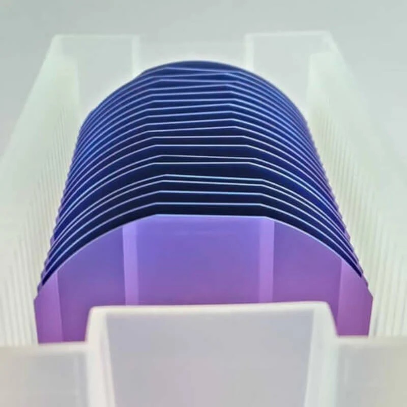
The 4-inch N-type silicon wafers are made of high-purity monocrystal silicon materials, doped with phosphorus (P) or arsenic (As) to form N-type conductive characteristics, and the resistivity range is strictly controlled within 10 to 20Ω·cm to ensure excellent carrier mobility. The wafer surface is covered with an oxide layer (SiO₂), usually 100-1000 nm thick, formed by thermal oxidation or chemical vapor deposition (CVD) process, providing excellent insulation and interface stability.
2. Technical parameters
Dimensions: 4 inches (100mm) diameter, 525±25μm thickness
Conduction type: N type (doped phosphorus/arsenic)
Resistivity: 10~20Ω·cm (uniformity ±5%)
Oxide thickness: customized (e.g. 300nm or 1000nm)
Crystal orientation: <100> or <111>, low defect density (<500 EPI)
Surface treatment: double-sided polishing (Ra <0.5nm) or single-sided oxidation
3. Core strengths
High purity silicon substrate: purity ≥99.9999%, reduce the impact of impurities on device performance.
Precise resistivity control: ensures a balance between low power consumption and high response speed.
Stable oxide layer: Enhanced insulation against leakage current, compatible with lithography and etching processes.
Strict quality control: According to ASTM F1241 and SEMI standards, tested by four-probe method (4PP) and elliptometer.
4. Technical details and innovation
Oxide layer process: Dry oxygen Oxidation (dry oxygen Oxidation) to generate dense SiO₂ layer, Wet oxygen oxidation (wet oxygen Oxidation) to improve the growth rate.
Doping technology: Ion implantation or diffusion method accurately controls the doping concentration and optimizes the carrier lifetime.
Surface passivation: The oxide layer reduces surface state density and improves device reliability and radiation resistance.
5. Market trends and demands
With the popularity of 5G communications, the Internet of Things (IoT) and new energy vehicles, the demand for high-performance silicon wafers has surged. 4-inch N-type wafers continue to play an important role in the field of low - and medium-power devices and research and development due to their high cost performance. The optimization of oxide layers, such as the silicon nitride composite layer, further extends its application in third-generation semiconductors, such as SiC epitaxy.
conclusion
4-inch N-type silicon wafers (10-20 Ω·cm resistivity) and oxide substrates are the core materials of the semiconductor industry, and their precision manufacturing and strict quality control provide a reliable basis for advanced electronic devices. Whether it is a research and development laboratory or a mass production line, the choice of suitable silicon solutions will significantly enhance the competitiveness of the product.