4-Inch P/N Type (100) Silicon Wafer with SiN Layer: Advanced Solutions for Semiconductor Innovation
Introduction: Elevating Semiconductor Performance with SiN Technology
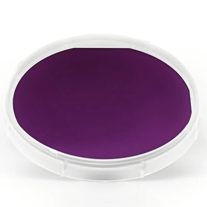
In semiconductor manufacturing, surface passivation and insulation are critical to device reliability and efficiency. The 4-inch P/N Type (100) Silicon Wafer integrated with a silicon nitride (SiN) layer offers a robust platform for high-power electronics, sensors, and optical systems. Combining the electrical advantages of P/N-type doping with SiN’s protective properties, this substrate addresses challenges in thermal management, contamination resistance, and long-term stability.
Core Specifications and Technical Features
Substrate Design
4-Inch Diameter (100mm): Optimized for R&D prototyping, small-batch production, and specialized applications.
P/N-Type Doping:
P-Type (Boron): Ideal for power MOSFETs, IGBTs, and high-voltage devices.
N-Type (Phosphorus/Arsenic): Suited for high-frequency transistors, sensors, and low-loss circuits.
(100) Crystal Orientation: Ensures uniform epitaxial growth and compatibility with standard fabrication processes.
Silicon Nitride (SiN) Layer
Deposition Method: Plasma-enhanced chemical vapor deposition (PECVD) for uniform, stress-controlled SiN coating.
Key Functions:
Surface Passivation: Reduces interface defects and prevents contamination during processing.
Insulation Barrier: High dielectric strength (≥10 MV/cm) isolates conductive layers in multi-stack devices.
Anti-Reflective Coating (ARC): Enhances light absorption in photovoltaics and photonic devices.
Why Choose This Silicon Wafer?
Dual Doping Flexibility: Select P- or N-type based on device polarity requirements.
Enhanced Reliability: SiN extends device longevity in high-power and corrosive conditions.
Process Compatibility: Integrates seamlessly with lithography, etching, and metallization workflows.
Customization: Adjust SiN thickness (50–500nm) or add patterned structures for specialized needs.
Conclusion: Driving Innovation in Power, MEMS, and Beyond
The 4-inch P/N Type (100) Silicon Wafer with SiN Layer is a transformative solution for modern semiconductor challenges. Its synergy of high-quality doping, crystal orientation, and multifunctional SiN coating empowers engineers to push the limits of efficiency and durability in power systems, sensors, and optoelectronic devices.
Unlock the potential of your next project with this cutting-edge, SiN-enhanced substrate!