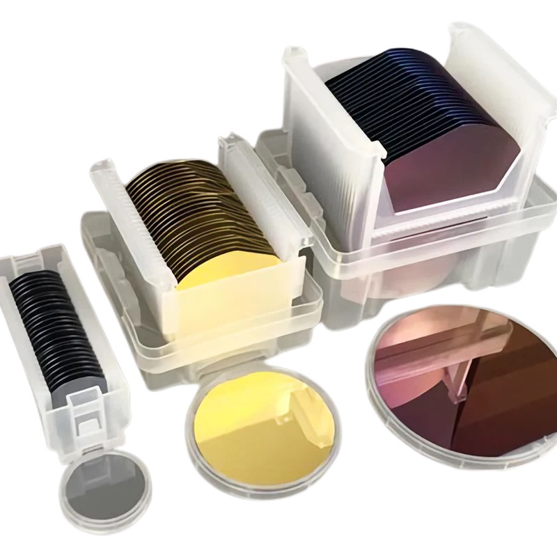
6-inch N-type (100) silicon wafers: Technical advantages and multi-field applications of 100nm silver coating
Introduction: Innovative fusion of high-performance substrates
With the rapid development of semiconductor and optoelectronic technology, the conductivity and surface functionality of substrate have become the core of device efficiency. By integrating 100nm silver (Ag) coatings, 6-inch N-type (100) silicon wafers combine high electron mobility and low resistance with silver's optical reflection advantages to provide innovative solutions for 5G communications, optoelectronics and biosensing. This paper deeply analyzes its technical specifications, application scenarios and core values.
Core specifications and technical highlights
Substrate parameter
6-inch diameter (150mm) : Suitable for mass production, balancing cost and productivity, widely used in integrated circuit and power device manufacturing.
N-type doping (phosphorus/arsenic doping) : high electron concentration (>10¹⁵ cm⁻³), support high-speed signal transmission and low power operation.
(100) Crystal orientation: uniform arrangement of surface atoms, compatible with mainstream CMOS process and gallium nitride (GaN) epitaxial growth.
100nm silver coating
Magnetron sputtering process: high purity (>99.99%), dense silver layer, thickness accuracy ±5nm, surface roughness (Ra) <2nm.
Dual function design:
Enhanced conductivity: The very low resistivity of silver (1.59×10⁻⁸Ω·m) reduces contact resistance and improves high-frequency signal integrity.
Optical reflection: the reflectance of visible light band is >95%, optimizing the light extraction efficiency of LED, laser and other photoelectric devices.
Why choose this silicon wafer?
Production level performance: The 6-inch size meets the needs of large-scale manufacturing such as automotive electronics and consumer electronics.
Multifunctional integration: A single substrate meets both electrical and optical design requirements, driving device miniaturization.
High reliability certification: complies with stringent standards such as AEC-Q101 (automotive) and JEDEC (electronic devices).
Customized services: Support silver layer patterning, multi-layer stacking (such as Ag/Cu/Ag) and other special process requirements.
Conclusion: Enabling future electronic and photonic technological innovation
** 6-inch N-type (100) silicon wafers (100nm silver coating) ** provide key technical support for high-frequency communications, efficient optoelectronics and precision sensing through innovative fusion of materials and processes. Whether it's developing the next generation of communications infrastructure or driving breakthroughs in biomedical detection technology, its high performance and versatility offer endless possibilities for engineers and researchers.
Inject new momentum into your technology blueprint with this cutting-edge substrate today!