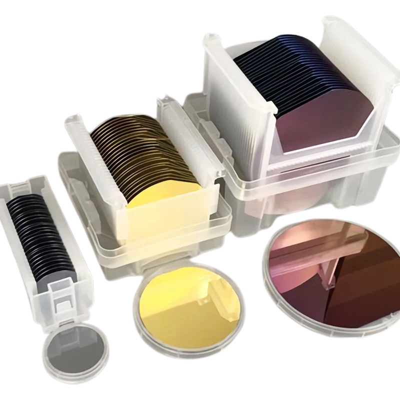
4-Inch N-Type (100) Silicon Wafer with Ultra-Low Resistivity (0.01~0.02Ω) and 100nm Gold Layer: High-Performance Solutions for Advanced Electronics
ntroduction: Precision Engineering for Demanding Applications
In high-frequency electronics and biomedical sensing, substrates must combine ultra-low resistance with exceptional surface stability. The 4-inch N-Type (100) Silicon Wafer, with a resistivity of 0.01~0.02Ω·cm and a 100nm gold (Au) layer, offers a premium solution for applications requiring minimal signal loss, corrosion resistance, and long-term reliability. This article explores its technical specifications, industry use cases, and competitive advantages.
Core Specifications and Technical Features
Substrate Design
4-Inch Diameter (100mm): Ideal for R&D prototyping, specialized device fabrication, and low-to-medium volume production.
N-Type Doping (Phosphorus/Arsenic): Ensures high electron mobility for fast signal transmission and low-power operation.
(100) Crystal Orientation: Provides a uniform surface for lithography and epitaxial growth, critical for CMOS and RF devices.
Ultra-Low Resistivity (0.01~0.02Ω·cm)
Near-metallic conductivity minimizes resistive losses in high-frequency circuits, power amplifiers, and quantum computing components.
Supports high-speed switching and reduces heat generation in compact designs.
100nm Gold (Au) Layer
Physical Vapor Deposition (PVD): Achieves a smooth, adhesive gold coating with high purity (>99.99%).
Dual Functionality:
Low-Contact Resistance: Gold’s exceptional conductivity (~2.44×10⁻⁸Ω·m) ensures reliable interconnects for high-frequency signals.
Bioinert Surface: Resists oxidation and corrosion, making it ideal for biomedical electrodes and implantable sensors.
Aerospace and Defense
Radar Systems: Combines high conductivity with thermal resilience for mission-critical applications.
Space-Grade Electronics: Meets MIL-STD-883 standards for reliability in harsh environments.
Advantages of the 100nm Gold Layer
Ultra-High Conductivity: Ensures minimal signal attenuation in GHz+ frequency ranges.
Chemical Stability: Gold resists tarnishing, even in humid or corrosive environments.
Biocompatibility: Safe for direct contact with biological tissues, critical for medical devices.
Thermal Management: Efficient heat dissipation prolongs device lifespan in power-intensive systems.
Why Choose This Silicon Wafer?
Performance-Driven Design: Ultra-low resistivity + gold layer maximizes efficiency in high-frequency and biomedical applications.
Industry Compliance: Adheres to AEC-Q101 (automotive) and ISO 13485 (medical) standards.
Customization Options: Adjust gold layer thickness (50–200nm) or add patterned structures (e.g., microelectrodes).
R&D to Production Scalability: Supports prototyping, pilot runs, and mid-scale manufacturing.
Conclusion: Redefining Excellence in High-Frequency and Biomedical Engineering
The 4-inch N-Type (100) Silicon Wafer with 0.01~0.02Ω·cm resistivity and 100nm gold layer sets a new benchmark for precision electronics and biomedical innovation. Its unique combination of ultra-low resistance, gold’s unmatched surface properties, and process adaptability makes it indispensable for engineers pushing the boundaries of 5G, quantum computing, and life sciences.
Upgrade your technology with this elite semiconductor substrate today!