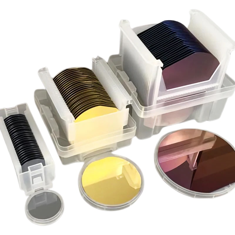
4-Inch N-Type (111) Silicon Wafer with 6~12Ω Resistivity and 100nm Silver Layer: Precision for Optoelectronics and Sensors
Introduction: Bridging Conductivity and Optical Performance
In the evolving landscape of optoelectronics and high-frequency devices, substrates must balance electrical performance with optical functionality. The 4-inch N-Type (111) Silicon Wafer, with a 6~12Ω·cm resistivity and a 100nm silver (Ag) layer, offers a unique synergy of conductivity, reflectivity, and process adaptability. This article delves into its technical specifications, applications, and why it stands out in precision-driven industries.
Core Specifications and Technical Highlights
Substrate Design
4-Inch Diameter (100mm): Optimized for R&D prototyping, specialized sensors, and low-volume production.
N-Type Doping (Phosphorus/Arsenic): Provides free electrons for high-speed signal transmission and low-loss applications.
(111) Crystal Orientation: Enhances epitaxial growth uniformity for optoelectronic devices like LEDs and photodetectors.
Resistivity Range (6~12Ω·cm)
Moderate resistivity balances conductivity and thermal stability, suitable for RF switches, microwave circuits, and sensor arrays.
Reduces parasitic capacitance in high-frequency designs.
100nm Silver (Ag) Layer
Sputtering/Evaporation Deposition: Ensures a smooth, adhesive silver coating with high reflectivity (>95% in visible spectrum).
Dual Functionality:
Conductive Layer: Lowers contact resistance for electrodes and interconnects.
Optical Reflector: Enhances light extraction in LEDs or acts as a mirror layer in photonic devices.
Advantages of the 100nm Silver Layer
Ultra-High Conductivity: Silver’s resistivity (~1.59×10⁻⁸Ω·m) outperforms most metals, reducing energy loss.
Optical Excellence: High reflectivity critical for light-emitting and sensing applications.
Corrosion Resistance: Silver’s inertness ensures long-term stability in harsh environments.
Thermal Conductivity: Efficient heat dissipation extends device lifespan in power-intensive systems.
Why Choose This Wafer?
Optoelectronic Optimization: Combines N-type (111) epitaxial readiness with silver’s optical properties.
Process Versatility: Compatible with lithography, etching, and thin-film deposition workflows.
Cost-Effective Reflectivity: Silver coating replaces gold in non-critical applications, lowering material costs.
Scalability: Supports niche R&D projects to pilot-scale production with consistent quality.
Conclusion: Redefining Precision in Optoelectronics and Beyond
The 4-inch N-Type (111) Silicon Wafer with 6~12Ω·cm resistivity and 100nm silver layer is a cornerstone for innovations requiring both electrical and optical precision. From energy-efficient lighting to next-gen sensors, its tailored design empowers engineers to achieve higher efficiency, miniaturization, and reliability.
Elevate your optoelectronic and high-frequency designs with this multifunctional substrate today!