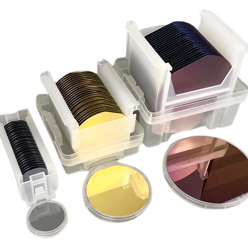
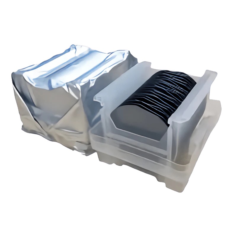
4-Inch P-Type (100) Silicon Wafer with Ultra-Low Resistivity (0.005~0.01Ω) and Nickel Layer: Technical Advantages and Applications
Introduction: The Fusion of Ultra-Low Resistivity and Metallization Technology
In the fields of power semiconductors and advanced packaging, substrate conductivity and metallization processes are critical to device efficiency and reliability. The 4-inch P-Type (100) Silicon Wafer, with its ultra-low resistivity of 0.005~0.01Ω·cm and nickel (Ni) layer coating, stands out as an ideal solution for high-current-density devices and miniaturized packaging. This article explores its core specifications, applications, and technical advantages.
Core Specifications and Technical Highlights
Substrate Parameters
4-Inch Diameter (100mm): Optimized for R&D, small-batch production, and specialized device manufacturing.
P-Type Doping (Boron): Hole-dominated conductivity enhances voltage tolerance and thermal stability in power devices.
(100) Crystal Orientation: Uniform lattice structure ensures compatibility with mainstream lithography and thin-film deposition processes.
Ultra-Low Resistivity (0.005~0.01Ω·cm)
Near-metallic conductivity minimizes conduction losses, ideal for IGBTs, MOSFETs, and fast-recovery diodes in high-power applications.
Supports high-temperature and high-frequency operations, reducing heat generation and improving energy efficiency.
Nickel (Ni) Layer Coating
Electroplating/Sputtering Process: Delivers a uniform, dense nickel layer (customizable thickness) to enhance surface conductivity and solderability.
Multifunctional Use: Serves as an electrode contact layer, electromagnetic shield, or diffusion barrier, improving device integration and longevity.
Advantages of the Nickel Layer Coating
Superior Conductivity: Nickel’s low resistivity (~6.9×10⁻⁸Ω·m) reduces contact resistance.
Corrosion Resistance: Protects the silicon substrate from oxidation and chemical degradation.
Process Compatibility: Supports wire bonding, flip-chip bonding, and other packaging techniques.
Cost Efficiency: Nickel coating replaces expensive metals (e.g., gold), lowering costs for high-frequency/high-power devices.
Why Choose This Silicon Wafer?
Peak Performance: Ultra-low resistivity + metallization pushes the power density limits of traditional silicon-based devices.
High Reliability: Nickel coating enhances mechanical strength and thermal cycling endurance, meeting automotive standards (e.g., AEC-Q101).
Customization: Tailored nickel layer thickness, surface roughness (Ra), and patterning available.
Rapid Deployment: Supports R&D to mid-scale production, accelerating time-to-market.
Conclusion: Empowering Next-Gen High-Power and High-Frequency Technologies
The 4-inch P-Type (100) Silicon Wafer (0.005~0.01Ω·cm with Nickel Layer) redefines solutions for high-power devices, advanced packaging, and miniaturized sensors through material and process innovation. Whether developing efficient energy conversion systems or exploring cutting-edge semiconductor technologies, its ultra-low resistivity and metallized functional layer are pivotal to achieving performance breakthroughs.
Upgrade your projects with this high-performance substrate today!