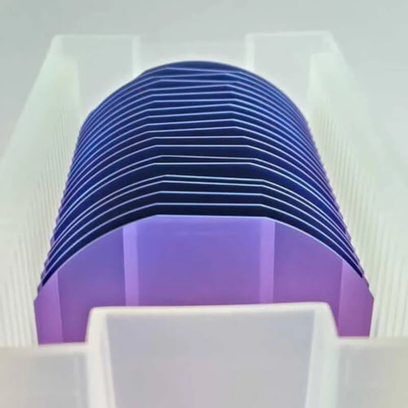
6-Inch N-Type (100/111) Single Side Polished Silicon Wafer: Technical Guide and Industry Applications
ntroduction
In semiconductor manufacturing, the choice of substrate material and surface finish directly impacts device performance. The 6-inch N-Type (100/111) Single Side Polished Silicon Wafer combines phosphorus/arsenic doping with a pristine polished surface and dual crystal orientations, offering engineers a versatile platform for cutting-edge electronics, sensors, and optoelectronics. This article explores its technical attributes, use cases, and advantages.
Key Specifications
Substrate Design
6-Inch Diameter (150mm): Ideal for mid-volume production of ICs, sensors, and research prototypes.
N-Type Doping (Phosphorus/Arsenic): Provides free electrons for high conductivity, suitable for high-speed and low-loss devices.
Crystal Orientation Options
(100) Orientation:
Preferred for CMOS, MOSFETs, and memory devices due to high electron mobility and compatibility with planar fabrication.
(111) Orientation:
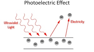
Offers superior surface atomic density for epitaxial growth, ideal for LEDs, laser diodes, and certain MEMS applications.
Single Side Polishing (SSP)
Ultra-smooth front surface (Ra <0.5nm) ensures precision in lithography and thin-film deposition.
Unpolished backside allows cost-effective handling or post-processing (e.g., back-grinding, metallization).
Why Choose This Wafer?
Dual Crystal Flexibility: Select (100) or (111) orientation based on device requirements.
High Surface Quality: SSP minimizes defects for high-yield device fabrication.
Cost Efficiency: Unpolished backside reduces material costs without compromising front-side performance.
Industry Compliance: Meets SEMI standards for thickness, flatness, and impurity levels.
Advantages of N-Type Doping
Lower Resistivity: Enables faster electron mobility compared to P-type substrates.
Radiation Hardness: Preferred for aerospace and high-reliability applications.
Thermal Stability: Maintains performance under high-temperature processing.
Conclusion
The 6-inch N-Type (100/111) Single Side Polished Silicon Wafer is a cornerstone for advanced semiconductor innovation. Whether developing high-frequency ICs, optoelectronic components, or MEMS sensors, its adaptable crystal orientations, pristine surface finish, and N-type conductivity make it indispensable for engineers and researchers.
Optimize your semiconductor workflows with this precision-engineered substrate today!