Introduction: The innovative value of high resistance silicon wafers
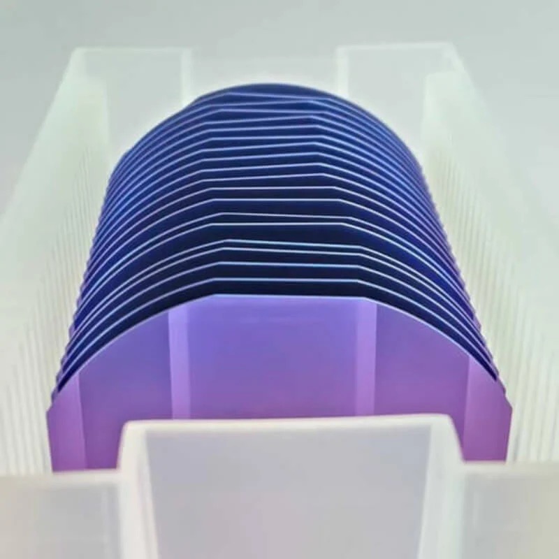
In semiconductor manufacturing, the resistivity of silicon wafer and the thickness of surface oxide layer directly affect the electrical performance and reliability of the device. 6-inch P-type (100) silicon wafers with medium to high resistivity of 20 to 50Ω and a thick oxide layer of 1000nm are ideal for high voltage power devices, sensors and optoelectronics. This paper analyzes its technical parameters, application scenarios and core advantages in detail.
Core specifications and design features
Substrate parameter
6 inch (150mm) diameter: suitable for medium to large scale semiconductor manufacturing with both productivity and cost.
(100) Crystal orientation: provides excellent carrier mobility and surface atomic arrangement, suitable for CMOS, photovoltaic and sensor processes.
P-type doping (boron doping) : Hole conduction characteristics optimize the voltage resistance and stability of power devices.
Resistivity range (20~50Ω·cm)
Medium and high resistivity design, reduce leakage current, suitable for high voltage insulated gate bipolar transistor (IGBT), power diode, etc.
Supports stable operation in high temperature and high power scenarios.
1000nm Thermal oxide (SiO₂)
The thick oxide layer provides superior insulation to meet the dielectric requirements of high-voltage devices above 10kV.
Surface passivation reduces interfacial state density and improves device lifetime and radiation resistance.
Why choose this silicon wafer?
High voltage compatibility: The 1000nm oxide layer breaks the traditional thickness limit and meets the requirements of the next generation of high voltage/high temperature devices.
Process flexibility: Support photolithography, etching, film deposition and other multi-step processing, compatible with industry standard production lines.
High reliability: Low defect density (<10 EPI/cm²) ensures device yield and meets automotive electronics and industrial standards.
Customization options: Single/double side polishing, local oxidation (LOCOS) and other process extensions are available.
Conclusion: The cornerstone of promoting high voltage and high power technology
** 6-inch P-type (100) silicon wafers (20 to 50Ω·cm, 1000nm oxide layer) ** are redefining the performance boundaries of power semiconductors and MEMS devices with their unique electrical properties and process adaptation. Whether developing efficient energy conversion systems or exploring miniaturized sensor technology, this substrate provides a solid technical support for engineers and researchers.
Explore this high-performance silicon wafer today to fuel your project with innovation!