Introduction
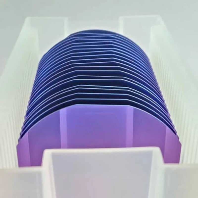
In semiconductor manufacturing, silicon wafers with tailored oxide layers are critical for achieving precise device performance. The 6-inch P-Type (100) Silicon Wafer with a 300nm oxide layercombines a boron-doped substrate and a uniform thermal oxide coating, making it indispensable for advanced electronics, sensors, and research. This article explores its technical specifications, applications, and advantages.
Key Specifications
Substrate Properties
6-Inch Diameter: Ideal for high-volume production of integrated circuits and MEMS devices.
P-Type (100) Crystal Orientation: Boron-doped for stable hole conductivity, optimized for MOSFETs and power devices.
300nm Oxide Layer
Thermally grown silicon dioxide (SiO₂) ensures uniformity and high dielectric strength.
Acts as an insulating layer, gate oxide, or protective coating in device fabrication.
Surface Quality
Ultra-flat polished surface (single/double side) minimizes defects in lithography and thin-film processes.
Research & Prototyping: Widely adopted in labs for studying oxide-semiconductor interfaces.
Advantages of the 300nm Oxide Layer
Thermal Stability: Withstands high-temperature processing steps in semiconductor fabrication.
Uniform Thickness: Ensures consistent electrical performance across the wafer.
Cost-Effective: Reduces post-processing steps by integrating a pre-grown oxide layer.
Why Choose This Wafer?
High Purity: Low defect density for reliable device yield.
Customization: Available with SSP/DSP finishes and tailored oxide thickness.
Industry Compliance: Meets standards for aerospace, automotive, and consumer electronics.
Conclusion
The 6-inch P-Type (100) Silicon Wafer with 300nm oxide layer is a cornerstone for modern semiconductor innovation. Its robust substrate, precision oxide coating, and adaptability to diverse applications make it a top choice for engineers and researchers aiming to push the boundaries of electronics and microfabrication.
Elevate your semiconductor projects with this advanced, oxide-integrated substrate!