Introduction
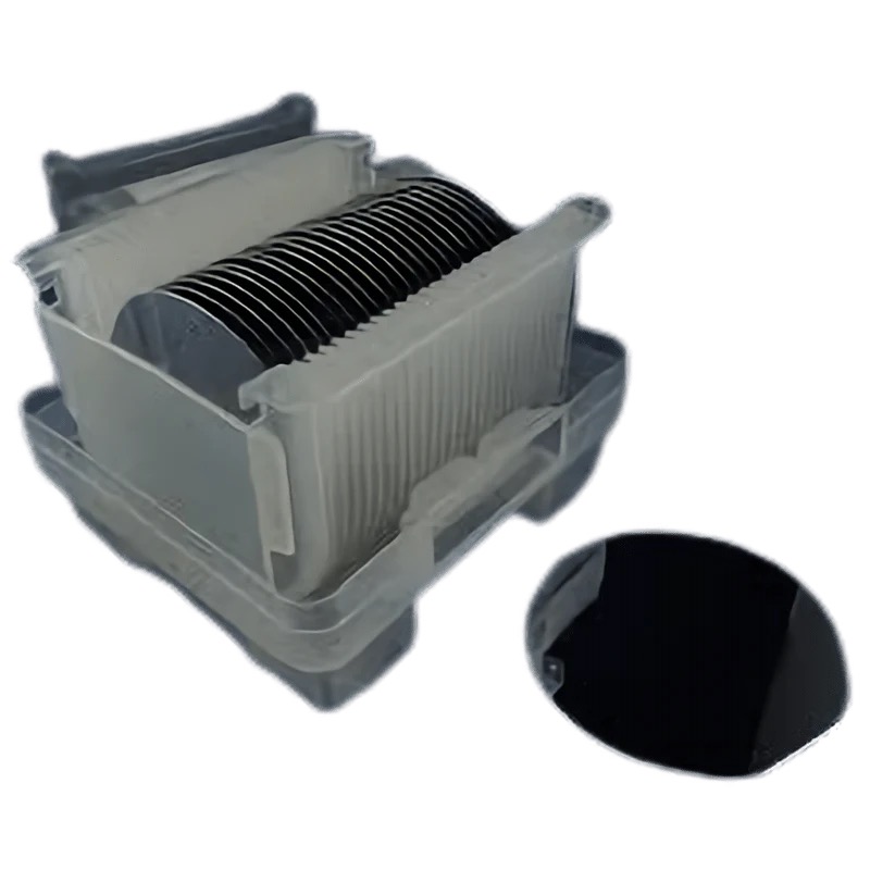
Silicon wafers are the backbone of modern electronics, serving as the foundation for integrated circuits, sensors, and photovoltaic devices. Among these, the 4-inch P/N Type (100) Silicon Wafer with a resistivity range of 1~5Ω and single/double side polishing stands out for its versatility and precision. This article breaks down its features, applications, and benefits for engineers, researchers, and manufacturers.
Key Features of the 4-Inch P/N Type (100) Wafer
Size and Crystal Orientation
4-Inch Diameter: A compact yet efficient size for prototyping, R&D, and small-scale production.
(100) Crystal Orientation: Offers optimal electronic properties for semiconductor devices like MOSFETs and LEDs.
Resistivity (1~5Ω)
Tailored resistivity ensures compatibility with both high-frequency and power device applications.
P-type (boron-doped) or N-type (phosphorus/arsenic-doped) options cater to specific circuit requirements.
Polishing Options
Single-Side Polished (SSP): Ideal for thin-film deposition and lithography processes.
Double-Side Polished (DSP): Ensures ultra-flat surfaces for advanced MEMS and optical applications.
Why Choose This Silicon Wafer?
High Purity: Minimizes defects for reliable device performance.
Customizable: Available in SSP/DSP finishes and tailored doping levels.
Cost-Efficient: Balances performance and affordability for diverse use cases.
Conclusion
The 4-inch P/N Type (100) Silicon Wafer with 1~5Ω resistivity is a critical tool for advancing semiconductor technology. Whether you’re developing cutting-edge electronics or conducting materials research, its precision polishing, crystal structure, and doping flexibility make it indispensable.