Introduction
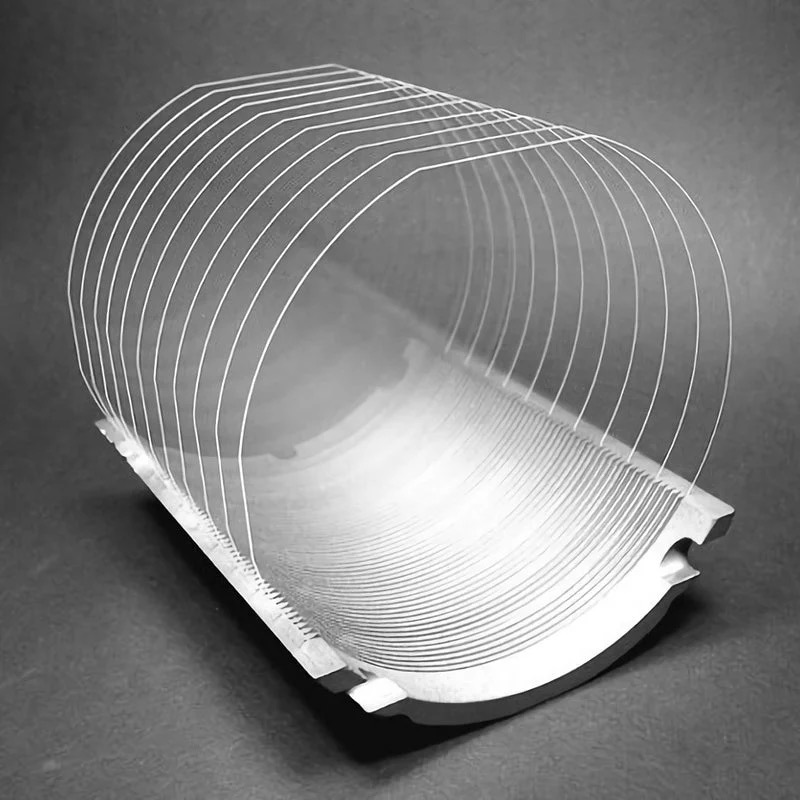
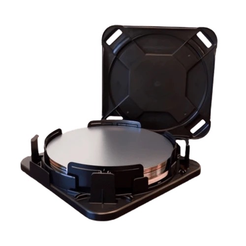
Combining the robustness of silicon with the optical clarity and thermal stability of Borofloat glass, 4-inch silicon wafers with a 300nm oxide layer offer a unique hybrid substrate for advanced semiconductor and microsystems applications. This article explores their design advantages, technical specifications, and suitability for MEMS, photonics, and sensing technologies.
Key Features
Borofloat Glass Substrate
Material Properties:
Low Thermal Expansion: Matches silicon’s thermal behavior, reducing stress in high-temperature processes.
Optical Clarity: High transparency in UV to IR spectra, ideal for optical and photonic devices.
Chemical Resistance: Withstands harsh etchants and solvents used in microfabrication.
Applications: Microfluidics, lab-on-chip systems, and optical windows.
300nm Silicon Oxide (SiO₂) Layer
Functionality:
Electrical Insulation: Isolates conductive layers in MEMS and ICs.
Surface Passivation: Protects silicon from contamination and oxidation.
Etching Mask: Enables precise patterning during lithography.
Compatibility: Integrates with CMOS, thin-film deposition, and dry/wet etching processes.
4-Inch Wafer Size
Balances surface area for prototyping and compatibility with smaller fabrication tools.
Cost-effective for small-batch production and research labs.
Advantages Over Conventional Substrates
Thermal Compatibility:
Borofloat’s thermal expansion coefficient (3.25 × 10⁻⁶/K) closely matches silicon, minimizing delamination risks.
Optical Performance:
Superior UV transmission compared to standard glass, enabling applications in spectroscopy and UV lithography.
Process Flexibility:
Compatible with silicon-based microfabrication (e.g., DRIE, sputtering) and glass-specific techniques (e.g., laser ablation).
Durability:
Resists mechanical and thermal shocks, suitable for harsh environments.
Selecting the Right Substrate
Optical Needs: Choose Borofloat for UV/IR transparency or light-guiding applications.
Electrical Requirements: Utilize the 300nm oxide layer for insulation or capacitive sensing.
Fabrication Compatibility: Verify etching and bonding processes align with Borofloat’s chemical resistance.
Conclusion
4-inch silicon wafers with 300nm oxide layers on Borofloat glass substrates bridge the gap between silicon’s electronic prowess and glass’s optical versatility. Their hybrid design supports MEMS, photonics, and biomedical devices, offering unmatched thermal stability, optical clarity, and fabrication flexibility. For projects demanding multifunctional substrates, this platform is a game-changer.
