Silicon Pattern Wafer 6~12 Inch: Core Substrate for Advanced Semiconductor Integrated Circuits
Introduction
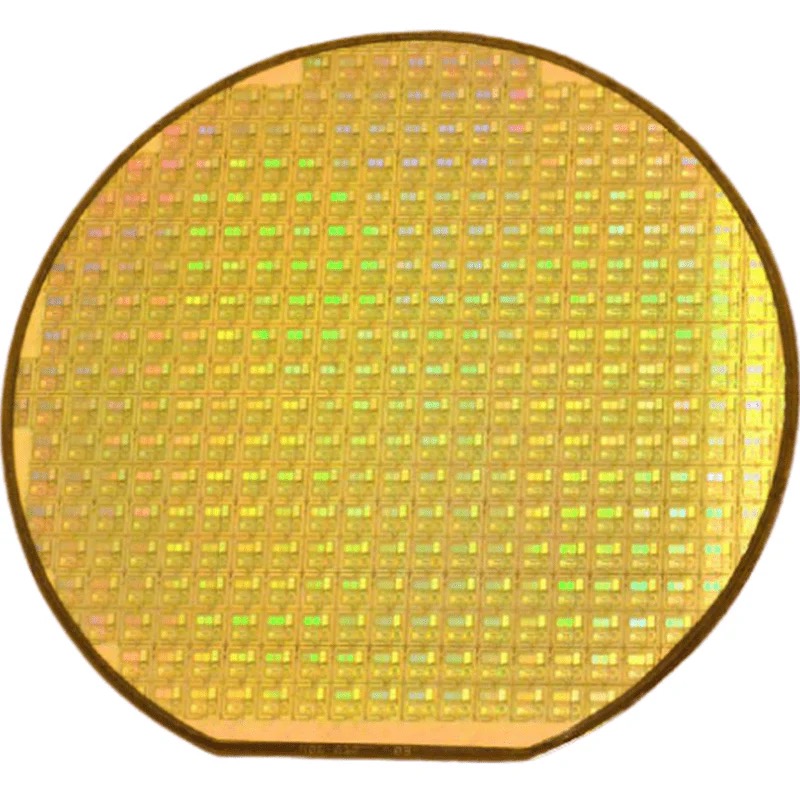
Silicon pattern wafers (6~12 inch) are foundational substrates in semiconductor manufacturing, enabling the fabrication of integrated circuits (ICs), micro-electromechanical systems (MEMS), and power devices. These wafers are pre-patterned with microstructures using advanced lithography techniques, serving as templates for high-precision device layering and alignment. With sizes ranging from 6-inch (150 mm) for specialized applications to 12-inch (300 mm) for mass production, they balance scalability, cost efficiency, and performance611.
Key Features of Silicon Pattern Wafers
Size Versatility
6-inch Wafers: Ideal for R&D, prototyping, and niche applications (e.g., sensors, optoelectronics) due to lower material costs and compatibility with legacy equipment6.
12-inch Wafers: Dominant in high-volume production (e.g., CPUs, memory chips), offering ~30% cost savings per die and superior uniformity for nanoscale patterning11.
Pattern Precision
Utilizes photolithography or electron-beam lithography to create sub-micron features, critical for transistors, interconnects, and MEMS structures8.
Advanced alignment techniques ensure multi-layer accuracy, reducing defects in 3D NAND and FinFET architectures11.
Material Quality
High-purity single-crystal silicon grown via the Czochralski (CZ) method minimizes defects and oxygen content6.
Oxide or nitride layers (e.g., SiO₂, SiN) are often integrated for insulation, passivation, or as hard masks during etching17.
Surface Treatment
Single-sided polishing (Ra < 0.5 nm) ensures smooth surfaces for lithography, while backside texturing may reduce warpage28.
Applications in Semiconductor Technology
Integrated Circuits (ICs)
CMOS Logic Chips: 12-inch wafers dominate CPU/GPU production, leveraging high-density patterning for 5 nm/3 nm nodes11.
Memory Devices: DRAM and 3D NAND flash rely on multi-layer stacking enabled by precise alignment6.
Power Electronics
Patterned wafers support high-voltage MOSFETs and IGBTs, with trench structures optimizing current flow and heat dissipation7.
MEMS and Sensors
6-inch wafers are cost-effective for accelerometers, gyroscopes, and pressure sensors, where patterned cavities and cantilevers enable mechanical functionality8.
Optoelectronics
Used in photonic ICs and LED arrays, with patterns guiding light propagation or forming waveguide structures11.
Manufacturing and Quality Control
Lithography Techniques
DUV/EUV Lithography: Enables sub-10 nm feature sizes for advanced nodes11.
Nanoimprint Lithography: Emerging for low-cost, high-throughput patterning in MEMS and sensors8.
Defect Mitigation
In-situ electron microscopy (e.g., SEM-CHIPNOVA) monitors pattern integrity during fabrication, detecting voids or misalignments in real time8.
Statistical process control (SPC) ensures resistivity uniformity (1~100 Ω·cm) and oxide layer consistency211.
Thermal and Mechanical Stability
Silicon’s low thermal expansion coefficient minimizes warpage during high-temperature processes like CVD or annealing7.
Market Trends and Innovations
Demand for Larger Wafers
Transition to 12-inch wafers accelerates for AI/5G chips, though 8-inch remains vital for IoT and automotive sensors67.
Advanced Materials Integration
Hybrid substrates (e.g., silicon-on-sapphire) enhance performance in RF and high-frequency applications1.
Cu/Si nanocomposites (as studied in PA6-Cu/Si research) may future improve wafer durability and thermal conductivity2.
Sustainability Focus
Recycling test-grade wafers and reducing chemical waste align with green semiconductor initiatives11.
Why Choose Silicon Pattern Wafers?
Scalability: Compatible with both legacy 6-inch fabs and cutting-edge 12-inch foundries.
Cost Efficiency: Larger wafers reduce per-die costs, while smaller sizes optimize R&D budgets611.
Versatility: Supports diverse technologies, from analog circuits to quantum dot devices8.
Conclusion
Silicon pattern wafers (6~12 inch) are indispensable in modern semiconductor ecosystems, enabling innovations from AI chips to wearable health monitors. Their precision, material quality, and adaptability ensure they remain central to advancements in CMOS scaling, MEMS miniaturization, and energy-efficient electronics.